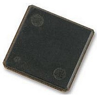
H5PS5162FFR-S6C HYNIX SEMICONDUCTOR, H5PS5162FFR-S6C Datasheet - Page 32

H5PS5162FFR-S6C
Manufacturer Part Number
H5PS5162FFR-S6C
Description
58T1896
Manufacturer
HYNIX SEMICONDUCTOR
Datasheet
1.H5PS5162FFR-S6C.pdf
(39 pages)
Specifications of H5PS5162FFR-S6C
Memory Type
SDRAM
Memory Configuration
32M X 16
Memory Case Style
FBGA
No. Of Pins
84
Operating Temperature Range
0°C To +85°C
Memory Size
512 Mbit
Voltage Vcc
1.8V
Rohs Compliant
Yes
Available stocks
Company
Part Number
Manufacturer
Quantity
Price
Company:
Part Number:
H5PS5162FFR-S6C
Manufacturer:
HYNIX
Quantity:
9 500
Company:
Part Number:
H5PS5162FFR-S6C
Manufacturer:
HYNIX
Quantity:
2 000
Company:
Part Number:
H5PS5162FFR-S6C
Manufacturer:
ST
Quantity:
40
Company:
Part Number:
H5PS5162FFR-S6C
Manufacturer:
HYNIX
Quantity:
4 000
Part Number:
H5PS5162FFR-S6C
Manufacturer:
HYNIX/海力士
Quantity:
20 000
1) For all input signals the total tIS(setup time) and tIH(hold) time) required is calculated by adding the
datasheet value to the derating value listed in above Table.
Setup(tIS) nominal slew rate for a rising signal is defined as the slew rate between the last crossing of
V
the slew rate between the last crossing of V
always earlier than the nominal slew rate for line between shaded ‘V
rate for derating value(see fig a.) If the actual signal is later than the nominal slew rate line anywhere
between shaded ‘V
to dc level is used for derating value(see Fig b.)
Hold(tIH) nominal slew rate for a rising signal is defined as the slew rate between the last crossing of
VIL(dc)max and the first crossing of V
slew rate between the last crossing of V
line between shaded ‘dc to V
signal is earlier than the nominal slew rate line anywhere between shaded ‘dc to V
rate of a tangent line to the actual signal from the dc level to V
d.)
Although for slow rates the total setup time might be negative(i.e. a valid input signal will not have reached
V
tion and reach V
For slew rates in between the values listed in table, the derating values may obtained by linear interpolation.
These values are typically not subject to production test. They are verified by design and characterization.
10. The maximum limit for this parameter is not a device limit. The device will operate with a greater value
for this parameter, but system performance (bus turnaround) will degrade accordingly.
11. MIN ( t CL, t CH) refers to the smaller of the actual clock LOW time and the actual clock HIGH time as
provided to the device (i.e. this value can be greater than the minimum specification limits for t CL and t CH).
For example, t CL and t CH are = 50% of the period, less the half period jitter ( t JIT(HP)) of the clock
source, and less the half period jitter due to crosstalk ( t JIT(crosstalk)) into the clock traces.
12. t QH = t HP – t QHS, where:
13. tDQSQ: Consists of data pin skew and output pattern effects, and p-channel to n-channel variation of the
output drivers as well as output slew rate mismatch between DQS/ DQS and associated DQ in any given
cycle.
14. t DAL = (nWR) + ( tRP/tCK):
For each of the terms above, if not already an integer, round to the next highest integer. tCK refers to the
application clock period. nWR refers to the t WR parameter stored in the MR.
Example: For DDR533 at t CK = 3.75 ns with t WR programmed to 4 clocks. tDAL = 4 + (15 ns / 3.75 ns)
clocks =4 +(4)clocks=8clocks.
Rev. 1.0 / July. 2008
REF
IH/IL
tHP = minimum half clock period for any given cycle and is defined by clock HIGH or clock LOW (tCH,tCL).
tQHS accounts for:
(dc) and the first crossing of V
(ac) at the time of the rising clock transition) a valid input signal is still required to complete the transi-
1) The pulse duration distortion of on-chip clock circuits; and
2) The worst case push-out of DQS on one transition followed by the worst case pull-in of DQ on the
next transition, both of which are, separately, due to data pin skew and output pattern effects, and
p-channel to n-channel variation of the output drivers.
IH/IL
REF
(ac).
(dc) to ac region’, the slew rate of a tangent line to the actual signal from the ac level
REF
(dc) region’, use nominal slew rate for derating value(see Fig.c) If the actual
IH
(ac)min. Setup(tIS) nominal slew rate for a falling signal is defined as
REF
REF
(dc). Hold(tIH) nominal slew rate for a falling signal is defined as the
(dc). If the actual signal is always later than the nominal slew rate
REF
(dc) and the first crossing of V
REF
(dc) level is used for derating value(see Fig
REF
(dc) to ac region’, use nominal slew
IL
(ac)max. If the actual signal is
H5PS5162FFR series
REF
(dc) region’, the slew
Release
32


