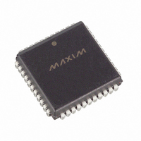
DS2151QNB Maxim Integrated Products, DS2151QNB Datasheet - Page 12

DS2151QNB
Manufacturer Part Number
DS2151QNB
Description
IC TXRX T1 1-CH 5V LP IND 44PLCC
Manufacturer
Maxim Integrated Products
Datasheet
1.DS2151QB.pdf
(60 pages)
Specifications of DS2151QNB
Function
Single-Chip Transceiver
Interface
T1
Number Of Circuits
1
Voltage - Supply
4.75 V ~ 5.25 V
Current - Supply
65mA
Operating Temperature
-40°C ~ 85°C
Mounting Type
Surface Mount
Package / Case
44-LCC, 44-PLCC
Includes
Alarm Detector and Generator, CSU Loop Codes Generator and Detector, DSX-1 and CSU Line Build-Outs Generator
Lead Free Status / RoHS Status
Contains lead / RoHS non-compliant
Power (watts)
-
TCR1: TRANSMIT CONTROL REGISTER 1 (Address = 35 Hex)
Note: For a detailed description of how the bits in TCR1 affect the transmit side formatter of the
DS2151Q, see
LOTCMC
(MSB)
SYMBOL
LOTCMC
TLINK
RBSE
TYEL
TCPT
GB7S
TFPT
TBL
Figure
TFPT
14-9.
POSITION
TCR1.7
TCR1.6
TCR1.5
TCR1.4
TCR1.3
TCR1.2
TCR1.1
TCR1.0
TCPT
NAME AND DESCRIPTION
Loss Of Transmit Clock Mux Control. Determines whether
the transmit side formatter should switch to the ever present
RCLK if the TCLK input should fail to transition
0 = do not switch to RCLK if TCLK stops
1 = switch to RCLK if TCLK stops
Transmit Framing Pass Through. (See note below.)
0 = Ft or FPS bits sourced internally
1 = Ft or FPS bits sampled at TSER during F-bit time
Transmit CRC Pass Through. (See note below.)
0 = source CRC6 bits internally
1 = CRC6 bits sampled at TSER during F-bit time
Robbed-Bit Signaling Enable. (See note below.)
0 = no signaling is inserted in any channel
1 = signaling is inserted in all channels (the TTR registers can
be used to block insertion on a channel by channel basis)
Global Bit 7 Stuffing. (See note below.)
0 = allow the TTR registers to determine which channels
containing all 0s are to be Bit 7 stuffed
1 = force Bit 7 stuffing in all 0 byte channels regardless of how
the TTR registers are programmed
TLINK Select. (See note below.)
0 = source FDL or Fs bits from TFDL register
1 = source FDL or Fs bits from the TLINK pin
Transmit Blue Alarm. (See note below.)
0 = transmit data normally
1 = transmit an unframed all 1s code at TPOS and TNEG
Transmit Yellow Alarm. (See note below.)
0 = do not transmit yellow alarm
1 = transmit yellow alarm
RBSE
12 of 60
GB7S
TLINK
TBL
(Figure
(LSB)
TYEL
1-1).


