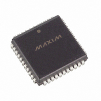
DS2151QNB Maxim Integrated Products, DS2151QNB Datasheet - Page 31

DS2151QNB
Manufacturer Part Number
DS2151QNB
Description
IC TXRX T1 1-CH 5V LP IND 44PLCC
Manufacturer
Maxim Integrated Products
Datasheet
1.DS2151QB.pdf
(60 pages)
Specifications of DS2151QNB
Function
Single-Chip Transceiver
Interface
T1
Number Of Circuits
1
Voltage - Supply
4.75 V ~ 5.25 V
Current - Supply
65mA
Operating Temperature
-40°C ~ 85°C
Mounting Type
Surface Mount
Package / Case
44-LCC, 44-PLCC
Includes
Alarm Detector and Generator, CSU Loop Codes Generator and Detector, DSX-1 and CSU Line Build-Outs Generator
Lead Free Status / RoHS Status
Contains lead / RoHS non-compliant
Power (watts)
-
RFDLM1: RECEIVE FDL MATCH REGISTER 1 (Address = 29 Hex)
RFDLM2: RECEIVE FDL MATCH REGISTER 2 (Address = 2A Hex)
When the byte in the Receive FDL Register matches either of the two Receive FDL Match Registers
(RFDLM1/RFDLM2), SR2.2 will be set to a 1 and the
7.2 Transmit Section
The transmit section will shift out into the T1 data stream, either the FDL (in the ESF framing mode) or
the Fs bits (in the D4 framing mode) contained in the Transmit FDL register (TFDL). When a new value
is written to the TFDL, it will be multiplexed serially (LSB first) into the proper position in the outgoing
T1 data stream. After the full 8 bits have been shifted out, the DS2151Q will signal the host
microcontroller that the buffer is empty and that more data is needed by setting the SR2.3 bit to a 1. The
If the TFDL is not updated, the old value in the TFDL will be transmitted once again.
The DS2151Q also contains a 0 stuffer that is controlled via the CCR2.4 bit. In both ANSI T1.403 and
TR54016, communications on the FDL follows a subset of a LAPD protocol. The LAPD protocol states
that no more than five 1s should be transmitted in a row so that the data does not resemble an opening or
closing flag (01111110) or an abort signal (11111111). If enabled via CCR2.4, the DS2151Q will
automatically look for five 1s in a row. If it finds such a pattern, it will automatically insert a 0 after the
five 1s. The CCR2.4 bit should always be set to a 1 when the DS2151Q is inserting the FDL. More on
how to use the DS2151Q in FDL and SLC-96 applications is covered in a separate application note.
TFDL: TRANSMIT FDL REGISTER (Address = 7E Hex)
The Transmit FDL Register (TFDL) contains the Facility Data Link (FDL) information that is to be
inserted on a byte basis into the outgoing T1 data stream in ESF mode. The LSB is transmitted first. In
D4 operation the TFDL can be the source of the Fs pattern. In this case a 1ch is written to the TFDL
register.
INT2
RFDL7
TFDL7
(MSB)
(MSB)
will also toggle low if enabled via IMR2.3. The user has 2ms to update the TFDL with a new value.
SYMBOL
SYMBOL
RFDL7
RFDL0
TFDL7
TFDL0
RFDL6
TFDL6
POSITION
POSITION
RFDL5
TFDL5
RFDL.7
RFDL.0
TFDL.7
TFDL.0
RFDL4
TFDL4
NAME AND DESCRIPTION
MSB of the FDL Match Code
LSB of the FDL Match Code
NAME AND DESCRIPTION
MSB of the FDL code to be transmitted
LSB of the FDL code to be transmitted
31 of 60
INT2
RFDL3
TFDL3
will go active if enabled via IMR2.2.
RFDL2
TFDL2
RFDL1
TFDL1
RFDL0
TFDL0
(LSB)
(LSB)


