CS8406-DZZ Cirrus Logic Inc, CS8406-DZZ Datasheet - Page 26
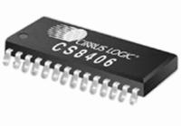
CS8406-DZZ
Manufacturer Part Number
CS8406-DZZ
Description
IC XMITTER DGTL 192KHZ 28TSSOP
Manufacturer
Cirrus Logic Inc
Type
Digital Audio Interface Transmitterr
Datasheet
1.CS8406-CZZ.pdf
(42 pages)
Specifications of CS8406-DZZ
Applications
Automotive Audio
Mounting Type
Surface Mount
Package / Case
28-TSSOP
Audio Control Type
Digital
Control Interface
3 Wire, Serial
Control / Process Application
AV & DVD Receivers, CD-R, Digital Mixing Consoles
Supply Voltage Range
3.14V To 5.25V
Lead Free Status / RoHS Status
Lead free / RoHS Compliant
For Use With
598-1017 - BOARD EVAL FOR CS8416 RCVR
Lead Free Status / RoHS Status
Lead free / RoHS Compliant, Lead free / RoHS Compliant
Other names
598-1722
Available stocks
Company
Part Number
Manufacturer
Quantity
Price

Part Number:
CS8406-DZZ
Manufacturer:
CIRRUS
Quantity:
20 000


26
VD
VL
GND
RST
H/S
TXN
TXP
OMCK
ISCLK
ILRCK
SDIN
SDA/CDOUT
SCL/CCLK
AD0/CS
AD1/CDIN
AD2
RXP
INT
TCBL
U
TSTN
23
22
24
25
26
21
13
12
14
28
27
19
15
20
6
9
1
2
3
4
5
Digital Power (Input) - Digital core power supply. Typically +3.3 V or +5.0 V.
Logic Power (Input) - Input/Output power supply. Typically +3.3 V or +5.0 V.
Ground (Input) - Ground for I/O and core logic.
Reset (Input) - When RST is low, the CS8406 enters a low power mode and all internal states are reset.
On initial power up, RST must be held low until the power supply is stable, and all input clocks are sta-
ble in frequency and phase. This is particularly true in Hardware Mode with multiple CS8406 devices,
where synchronization between devices is important.
Hardware/Software Control Mode Select (Input) -Determines the method of controlling the operation
of the CS8406, and the method of accessing CS and U data. In Software Mode, device control and CS
and U data access is primarily through the control port, using a microcontroller. To select Software
Mode, this pin should be permanently tied to GND.
Differential Line Drivers (Output) - These pins transmit biphase encoded data. The drivers are pulled
low while the CS8406 is in the reset state.
Master Clock (Input) - The frequency can be set through the control port registers.
Serial Audio Bit Clock (Input/Output) - Serial bit clock for audio data on the SDIN pin.
Serial Audio Input Left/Right Clock (Input/Output) - Word rate clock for the audio data on the SDIN
pin.
Serial Audio Data Port (Input) - Audio data serial input pin.
Serial Control Data I/O (I²C Mode) / Data Out (SPI) (Input/Output) - In I²C Mode, SDA is the control
I/O data line. SDA is open drain and requires an external pull-up resistor to VL. In SPI Mode, CDOUT is
the output data from the control port interface on the CS8406
Control Port Clock (Input) - Serial control interface clock and is used to clock control data bits into and
out of the CS8406. In I²C Mode, SCL requires an external pull-up resistor to VL.
Address Bit 0 (I²C Mode) / Control Port Chip Select (SPI) (Input) - A falling edge on this pin puts the
CS8406 into SPI Control Port Mode. With no falling edge, the CS8406 defaults to I²C Mode. In I²C
Mode, AD0 is a chip address pin. In SPI Mode, CS is used to enable the control port interface on the
CS8406
Address Bit 1 (I²C Mode) / Serial Control Data in (SPI) (Input) - In I²C Mode, AD1 is a chip address
pin. In SPI Mode, CDIN is the input data line for the control port interface.
Address Bit 2 (I²C Mode) (Input) - Determines the AD2 address bit for the control port in I²C Mode,
and should be connected to GND or VL. If SPI Mode is used, the AD2 pin should be connected to either
GND or VL.
Auxiliary AES3 Receiver Port (Input) - Input for an alternate, already AES3 coded, audio data source.
Interrupt (Output) - Indicates key events during the operation of the CS8406. All bits affecting INT may
be unmasked through bits in the control registers. Indication of the condition(s) that initiated an interrupt
are readable in the control registers. The polarity of the INT output, as well as selection of a standard or
open drain output, is set through a control register. Once set true, the INT pin goes false only after the
interrupt status registers have been read and the interrupt status bits have returned to zero.
Transmit Channel Status Block Start (Input/Output) - When operated as output, TCBL is high during
the first sub-frame of a transmitted channel status block, and low at all other times. When operated as
input, driving TCBL high for at least three OMCK clocks will cause the next transmitted sub-frame to be
the start of a channel status block.
User Data (Input) - May optionally be used to input User data for transmission by the AES3 transmitter,
see
pin. If the U pin is driven by a logic level output, a 100 Ω series resistor is recommended.
Test In (Input) - This pin is an input used for test purposes. It must be tied to ground for normal operation.
Figure 4
for timing information. If not driven, a 47 kΩ pull-down resistor is recommended for the U
CS8406
DS580F5
Related parts for CS8406-DZZ
Image
Part Number
Description
Manufacturer
Datasheet
Request
R

Part Number:
Description:
IC XMITTER DGTL 192KHZ 28SOIC
Manufacturer:
Cirrus Logic Inc
Datasheet:

Part Number:
Description:
IC XMITTER DGTL 192KHZ 28TSSOP
Manufacturer:
Cirrus Logic Inc
Datasheet:

Part Number:
Description:
IC, DIGITAL AUDIO TRANSMITTER, SOIC-28
Manufacturer:
Cirrus Logic Inc
Datasheet:

Part Number:
Description:
Transceiver IC
Manufacturer:
Cirrus Logic Inc
Datasheet:
Part Number:
Description:
IC,Digital Audio Transmitter,CMOS,TSSOP,28PIN,PLASTIC
Manufacturer:
Cirrus Logic Inc
Datasheet:
Part Number:
Description:
IC,Digital Audio Transmitter,CMOS,SOP,28PIN,PLASTIC
Manufacturer:
Cirrus Logic Inc
Datasheet:
Part Number:
Description:
IC,Digital Audio Transmitter,CMOS,TSSOP,28PIN,PLASTIC
Manufacturer:
Cirrus Logic Inc
Datasheet:

Part Number:
Description:
Audio DSPs IC 192 kHz Digital Audio Transmitter
Manufacturer:
Cirrus Logic Inc
Datasheet:
Part Number:
Description:
192 KHZ INDUSTRIAL DIGITAL AUDIO TRANSMITTER AUTOMOTIVE
Manufacturer:
Cirrus Logic Inc

Part Number:
Description:
Development Kit
Manufacturer:
Cirrus Logic Inc
Datasheet:
Part Number:
Description:
Development Kit
Manufacturer:
Cirrus Logic Inc
Datasheet:


Part Number:
Description:
Ref Bd For Speakerbar MSA & DSP Products
Manufacturer:
Cirrus Logic Inc