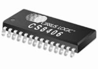
CS8406-DZZ Cirrus Logic Inc, CS8406-DZZ Datasheet - Page 33

CS8406-DZZ
Manufacturer Part Number
CS8406-DZZ
Description
IC XMITTER DGTL 192KHZ 28TSSOP
Manufacturer
Cirrus Logic Inc
Type
Digital Audio Interface Transmitterr
Datasheet
1.CS8406-CZZ.pdf
(42 pages)
Specifications of CS8406-DZZ
Applications
Automotive Audio
Mounting Type
Surface Mount
Package / Case
28-TSSOP
Audio Control Type
Digital
Control Interface
3 Wire, Serial
Control / Process Application
AV & DVD Receivers, CD-R, Digital Mixing Consoles
Supply Voltage Range
3.14V To 5.25V
Lead Free Status / RoHS Status
Lead free / RoHS Compliant
For Use With
598-1017 - BOARD EVAL FOR CS8416 RCVR
Lead Free Status / RoHS Status
Lead free / RoHS Compliant, Lead free / RoHS Compliant
Other names
598-1722
Available stocks
Company
Part Number
Manufacturer
Quantity
Price
Part Number:
CS8406-DZZ
Manufacturer:
CIRRUS
Quantity:
20 000
DS580F5
12.APPLICATIONS
12.1
12.2
12.3
12.4
Reset, Power Down and Start-Up
When RST is low, the CS8406 enters a low power mode and all internal states are reset, including the con-
trol port and registers, and the outputs are disabled. In Software Mode when RST is high, the control port
becomes operational and the desired settings should be loaded into the control registers. Writing a 1 to the
RUN bit will then cause the part to leave the low power state and begin operation. In Hardware Mode when
RST is high, the part will automatically leave the low power state and begin operation.
ID Code and Revision Code
The CS8406 has a register that contains a four-bit code to indicate that the addressed device is a CS8406.
This is useful when other CS84XX family members are resident in the same or similar systems, allowing
common software modules.
The CS8406 four-bit revision level code is also available. This allows the software driver for the CS8406 to
identify which revision of the device is in a particular system, and modify its behavior accordingly. To allow
for future revisions, it is strongly recommended that the revision code is read into a variable area within the
microcontroller, and used wherever appropriate as revision details become known.
Power Supply, Grounding, and PCB layout
The CS8406 operates from a VD = +3.3 V or +5.0 V and VL = +3.3 V or +5.0 V supply. These supplied may
be set independently. Follow normal supply decoupling practices, see
plies should be decoupled with a 0.1 μ F capacitor to GND to minimize AES3 transmitter induced transients.
Extensive use of power and ground planes, ground plane fill in unused areas and surface mount decoupling
capacitors are recommended. Decoupling capacitors should be mounted on the same side of the board as
the CS8406 to minimize inductance effects, and all decoupling capacitors should be as close to the CS8406
as possible.
The CS8406 is available in the compact QFN package. The underside of the QFN package reveals a metal
pad; this pad must mate with an equally dimensioned copper pad on the PCB and must be electrically con-
nected to ground. A series of vias should be used to connect this copper pad to one or more ground planes
on other PCB layers.
Synchronization of Multiple CS8406s
The AES3 transmitters of multiple CS8406s can be synchronized if all devices share the same master clock,
TCBL, and RST signals. The TCBL pin is used to synchronize multiple CS8406 AES3 transmitters at the
channel status block boundaries. One CS8406 must have its TCBL set to master; the others must be set to
slave TCBL. Alternatively, TCBL can be derived from external logic, whereby all CS8406 devices should be
set to slave TCBL.
Figures 5
and 6. The VD and VL sup-
CS8406
33


