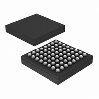
TDA9989ET/C1,551 NXP Semiconductors, TDA9989ET/C1,551 Datasheet - Page 36

TDA9989ET/C1,551
Manufacturer Part Number
TDA9989ET/C1,551
Description
IC HDMI TX 1.3A 150MHZ 64-TFBGA
Manufacturer
NXP Semiconductors
Type
Transmitterr
Datasheet
1.TDA9989ETC1518.pdf
(48 pages)
Specifications of TDA9989ET/C1,551
Applications
Cameras, Cell Phones, Media Players
Mounting Type
Surface Mount
Package / Case
64-TFBGA
Lead Free Status / RoHS Status
Lead free / RoHS Compliant
Other names
935288146551
Available stocks
Company
Part Number
Manufacturer
Quantity
Price
Company:
Part Number:
TDA9989ET/C1,551
Manufacturer:
NXP Semiconductors
Quantity:
10 000
NXP Semiconductors
Table 30.
T
[1]
[2]
13. Dynamic characteristics
Table 31.
T
TDA9989_2
Product data sheet
Symbol
5 V tolerant input pin HPD
V
V
C
CMOS 1.8 V and CMOS 3.3 V tolerant digital input/output pin INT_HDMI
V
V
V
5 V tolerant master bus: DDC-bus pins DSDA, DSCL
V
V
V
1.8 V to 3.3 V tolerant slave bus: I
V
V
V
CEC input/output
V
V
V
V
V
TMDS output pins: TX0 , TX0+, TX1 , TX1+, TX2 , TX2+, TXC and TXC+
V
V
Symbol
Clock input: pin VCLK
f
t
t
f
clk(max)
su(D)
h(D)
clk
amb
amb
clk
IL
IH
IL
IH
OL
OL
IL
IH
OL
IL
IH
OL
OH
IL
IH
hys(i)
O(dif)
O(cm)
i
See
For information, input hysteresis is normally supplied by the microprocessor input circuit: in this circumstance, external hysteresis
circuitry is not needed.
= 20 C to +85 C; unless otherwise specified.
= 20 C to +85 C; unless otherwise specified.
Section 7.1
Digital inputs and outputs
Timing characteristics
Parameter
LOW-level input voltage
HIGH-level input voltage
input capacitance
LOW-level input voltage
HIGH-level input voltage
LOW-level output voltage C
LOW-level output voltage
LOW-level input voltage
HIGH-level input voltage
LOW-level output voltage
LOW-level input voltage
HIGH-level input voltage
LOW-level output voltage
HIGH-level output voltage
LOW-level input voltage
HIGH-level input voltage
input hysteresis voltage
differential output voltage R
common-mode output
voltage
Parameter
maximum clock frequency
data input set-up time
data input hold time
clock duty cycle
clock frequency
[2]
and refer to the I
pin
2
C-bus specification version 2.1 (document order number 9398 393 40011).
2
C-bus input/output pins CSCL, CSDA
…continued
Conditions
-
-
-
-
R
L
EXT_SWING
EXT_SWING
Conditions
-
see
see
positive edge
CEC
= 10 pF; I
Figure 18
Figure 18
Rev. 02 — 11 June 2009
= 10 k
= 10 k
OL
[1]
= 2 mA
and
and
19
19
1 %
1 %
[1]
HDMI 1.3a transmitter with CEC support
[1]
[2]
Min
-
1.5
1
30
-
Min
0
2
-
0
1.4
0
0
0
1.4
0
0
1.4
0
2.5
0
2.5
-
400
-
Typ
-
-
-
50
12
Typ
-
-
4.5
-
-
-
-
-
-
-
-
-
-
-
-
-
0.27
514
3.05
TDA9989
Max
150
-
-
70
50
© NXP B.V. 2009. All rights reserved.
Max
0.8
-
-
0.85
-
0.4
0.4
0.6
5.5
0.4
0.6
5.5
0.4
3.6
0.60
3.6
-
600
-
Unit
MHz
ns
ns
%
MHz
Unit
V
V
pF
V
V
V
V
V
V
V
V
V
V
V
V
V
V
mV
V
36 of 48


