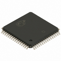
CY7C4841-10AC Cypress Semiconductor Corp, CY7C4841-10AC Datasheet - Page 15

CY7C4841-10AC
Manufacturer Part Number
CY7C4841-10AC
Description
IC SYNC FIFO 4KX9X2 64LQFP
Manufacturer
Cypress Semiconductor Corp
Series
CY7Cr
Datasheet
1.CY7C4811-10AC.pdf
(23 pages)
Specifications of CY7C4841-10AC
Function
Synchronous, Dual Port
Memory Size
72K (4K x 9 x 2)
Data Rate
100MHz
Access Time
8ns
Voltage - Supply
3.3V
Operating Temperature
-40°C ~ 85°C
Mounting Type
Surface Mount
Package / Case
64-LQFP
Density
64Kb
Word Size
9b
Sync/async
Synchronous
Expandable
Yes
Package Type
TQFP
Operating Supply Voltage (typ)
5V
Operating Supply Voltage (min)
4.5V
Operating Supply Voltage (max)
5.5V
Operating Temp Range
0C to 70C
Operating Temperature Classification
Commercial
Mounting
Surface Mount
Pin Count
64
Lead Free Status / RoHS Status
Contains lead / RoHS non-compliant
Other names
428-1259
Available stocks
Company
Part Number
Manufacturer
Quantity
Price
Company:
Part Number:
CY7C4841-10AC
Manufacturer:
CYPRESS
Quantity:
220
Programmable Flag (PAEA,PAEB, PAFA,PAFB) Operation
Whether the flag offset registers are programmed as de-
scribed in Table 1 or the default values are used, the programmable
almost-empty flag (PAEA,PAEB) and programmable almost-full flag
(PAFA,PAFB) states are determined by their corresponding offset
registers and the difference between the read and write pointers.
Table 1. Writing the Offset Registers.
Notes:
Document #: 38-06005 Rev. **
24. The same selection sequence applies to reading form the registers. REN1 and REN2 are enabled and a read is performed on the LOW- to-HIGH transition of
LD
0
0
1
1
RCLK.
WEN
0
1
0
1
WCLK
8
8
8
8
8
8
8
8
[24]
256 x 9 x 2
Empty Offset (LSB) Reg.
Default Value = 007h
Full Offset (LSB) Reg
Default Value = 007h
Empty Offset (LSB) Reg.
Default Value = 007h
7
7
7
7
Full Offset (LSB) Reg
Default Value = 007h
2K x 9 x 2
Empty Offset (LSB)
Empty Offset (MSB)
Full Offset (LSB)
Full Offset (MSB)
No Operation
Write Into FIFO
No Operation
2
2
(MSB)
(MSB)
000
000
Figure 1. Offset Register Location and Default Values.
Selection
0
0
0
0
0
0
0
0
8
8
8
8
8
8
8
8
512 x 9 x 2
Empty Offset (LSB) Reg.
Default Value = 007h
Full Offset (LSB) Reg
Default Value = 007h
Empty Offset (LSB) Reg.
Default Value = 007h
Full Offset (LSB) Reg
Default Value = 007h
7
7
7
7
4K x 9 x 2
3
3
(MSB)
(MSB)
0000
0000
1
1
The number formed by the empty offset least significant bit
register and empty offset most significant register is referred
to as n and determines the operation of (PAEA,PAEB).
(PAEA,PAEB) is synchronized to the LOW-to-HIGH transition of
RCLK by one flip-flop and is LOW when the FIFO contains n or fewer
unread words. (PAEA,PAEB) is set HIGH by the LOW-to-HIGH tran-
sition of RCLK when the FIFO contains (n+1) or greater unread
words.
The number formed by the full offset least significant bit regis-
ter and full offset most significant bit register is referred to as
m and determines the operation of (PAFA,PAFB). (PAEA,PAEB) is
synchronized to the LOW-to-HIGH transition of (WCLKA,WCLKB) by
one flip-flop and is set LOW when the number of unread words in the
FIFO is greater than or equal to CY7C4801 (256–m), CY7C4811
(512–m), CY7C4821 (1K–m), CY7C4831 (2K–m), CY7C4841
(4K–m), and CY7C4851 (8K–m). (PAFA,PAFB) is set HIGH by the
LOW-to-HIGH transition of (WCLKA,WCLKB) when the number of
available memory locations is greater than m.
(MSB)
(MSB)
0
0
0
0
0
0
0
0
0
0
8
8
8
8
8
8
8
8
Empty Offset (LSB) Reg.
Default Value = 007h
Full Offset (LSB) Reg
Default Value = 007h
1K x 9 x 2
7
7
Empty Offset (LSB) Reg.
Default Value = 007h
Full Offset (LSB) Reg
Default Value = 007h
7
7
8K x 9 x 2
CY7C4831/4841/4851
CY7C4801/4811/4821
4
4
1
1
(MSB)
(MSB)
00000
00000
(MSB)
(MSB)
00
00
0
0
0
0
0
0
0
0
Page 15 of 23


