CY7C4841-10AC Cypress Semiconductor Corp, CY7C4841-10AC Datasheet - Page 7
CY7C4841-10AC
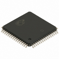
Manufacturer Part Number
CY7C4841-10AC
Description
IC SYNC FIFO 4KX9X2 64LQFP
Manufacturer
Cypress Semiconductor Corp
Series
CY7Cr
Datasheet
1.CY7C4811-10AC.pdf
(23 pages)
Specifications of CY7C4841-10AC
Function
Synchronous, Dual Port
Memory Size
72K (4K x 9 x 2)
Data Rate
100MHz
Access Time
8ns
Voltage - Supply
3.3V
Operating Temperature
-40°C ~ 85°C
Mounting Type
Surface Mount
Package / Case
64-LQFP
Density
64Kb
Word Size
9b
Sync/async
Synchronous
Expandable
Yes
Package Type
TQFP
Operating Supply Voltage (typ)
5V
Operating Supply Voltage (min)
4.5V
Operating Supply Voltage (max)
5.5V
Operating Temp Range
0C to 70C
Operating Temperature Classification
Commercial
Mounting
Surface Mount
Pin Count
64
Lead Free Status / RoHS Status
Contains lead / RoHS non-compliant
Other names
428-1259
Available stocks
Company
Part Number
Manufacturer
Quantity
Price
Company:

Part Number:
CY7C4841-10AC
Manufacturer:
CYPRESS
Quantity:
220


Switching Waveforms
Document #: 38-06005 Rev. **
Write Cycle Timing
Read Cycle Timing
RCLKA (RCLKB)
RENA1,RENA2
(RENB1,RENB2)
EFA(EFB)
QA
(QB
OEA(OEB)
WCLKA,WCLKB
WENA1(WENB1)
WENA2(WENB2)
WCLKA (WCLKB)
DA
(DB
WENA1
(WENB1)
WENA2(WENB2)
(if applicable)
FFA (FFB)
RCLKA (RCLKB)
RENA1,RENB2
(RENB1, RENB2)
Notes:
10. t
11. t
0
0
0
0
QA
cycle. If the time between the rising edge of (RCLKA,RCLKB) and the rising edge of (WCLKA,WCLKB) is less than t
next (WCLKA,WCLKB) rising edge.
cycle. It the time between the rising edge of (WCLKA,WCLKB) and the rising edge of RCLK is less than t
(RCLKA,RCLKB) rising edge.
DA
DB
QB
SKEW1
SKEW1
8
8
8
8
)
)
is the minimum time between a rising (RCLKA,RCLKB) edge and a rising (WCLKA,WCLKB) edge to guarantee that (FFA,FFB) will go HIGH during the current clock
is the minimum time between a rising (WCLKA,WCLKB) edge and a rising (RCLKA,RCLKB) edge to guarantee that (EFA,EFB) will go HIGH during the current clock
t
ENS
t
OLZ
t
SKEW1
t
ENH
t
t
CLKH
CLKH
[10]
t
t
t
A
REF
WFF
t
OE
t
t
CLK
CLK
t
SKEW1
NO OPERATION
[11]
t
t
DS
CLKL
t
CLKL
t
ENS
SKEW1
VALID DATA
t
DH
t
ENH
, then (EFA,EFB) may not change state until the next
t
REF
t
WFF
SKEW1
t
, then (FFA,FFB) may not change state until the
CY7C4831/4841/4851
OHZ
CY7C4801/4811/4821
NO OPERATION
NO OPERATION
Page 7 of 23
48X1–7
48X1–6
Related parts for CY7C4841-10AC
Image
Part Number
Description
Manufacturer
Datasheet
Request
R

Part Number:
Description:
Manufacturer:
Cypress Semiconductor Corp
Datasheet:
Part Number:
Description:
Manufacturer:
Cypress Semiconductor Corp
Datasheet:
Part Number:
Description:
Manufacturer:
Cypress Semiconductor Corp
Datasheet:
Part Number:
Description:
Manufacturer:
Cypress Semiconductor Corp
Datasheet:
Part Number:
Description:
Manufacturer:
Cypress Semiconductor Corp
Datasheet:
Part Number:
Description:
Manufacturer:
Cypress Semiconductor Corp
Datasheet:
Part Number:
Description:
Manufacturer:
Cypress Semiconductor Corp
Datasheet: