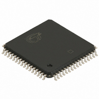
CY7C4841-10AC Cypress Semiconductor Corp, CY7C4841-10AC Datasheet - Page 19

CY7C4841-10AC
Manufacturer Part Number
CY7C4841-10AC
Description
IC SYNC FIFO 4KX9X2 64LQFP
Manufacturer
Cypress Semiconductor Corp
Series
CY7Cr
Datasheet
1.CY7C4811-10AC.pdf
(23 pages)
Specifications of CY7C4841-10AC
Function
Synchronous, Dual Port
Memory Size
72K (4K x 9 x 2)
Data Rate
100MHz
Access Time
8ns
Voltage - Supply
3.3V
Operating Temperature
-40°C ~ 85°C
Mounting Type
Surface Mount
Package / Case
64-LQFP
Density
64Kb
Word Size
9b
Sync/async
Synchronous
Expandable
Yes
Package Type
TQFP
Operating Supply Voltage (typ)
5V
Operating Supply Voltage (min)
4.5V
Operating Supply Voltage (max)
5.5V
Operating Temp Range
0C to 70C
Operating Temperature Classification
Commercial
Mounting
Surface Mount
Pin Count
64
Lead Free Status / RoHS Status
Contains lead / RoHS non-compliant
Other names
428-1259
Available stocks
Company
Part Number
Manufacturer
Quantity
Price
Company:
Part Number:
CY7C4841-10AC
Manufacturer:
CYPRESS
Quantity:
220
Bidirectional Configuration
The two FIFOs of the CY7C4801/4811/4821/4831/4841/4851
can be used to buffer data flow in two directions. In the exam-
ple that follows, processor A can write data to processor B via
Depth Expansion
CY7C4801/4811/4821/4831/4841/4851can be adapted to ap-
plications that require greater than 256/512/1024/2048/4096/
8192 words. The existence of dual enable pins on the read and
write ports allow depth expansion. The Write Enable 2/Load
(WENA2, WENB2) pins are used as a second write enables in
a depth expansion configuration, thus the Programmable flags
are set to the default values. Depth expansion is possible by
using one enable input for system control while the other en-
able input is controlled by expansion logic to direct the flow of
Document #: 38-06005 Rev. **
PROCESSOR A
CONTROL
ADDRESS
RAM
CLOCK
DATA
9
9
Figure 4. Block Diagram of Bidirectional Configuration.
V
CC
9
9
WENA2
WCLKA
WENA1
DA
RCLKB
RENB1
OEB
QB
RENB2
RAM ARRAY B
RAM ARRAY A
0
0
CY7C4851
DA
CY7C4801
CY7C4811
CY7C4821
CY7C4831
CY7C4841
QB
8
8
QA
DB
WENB1
WCLKB
WENB2
RENA2
RCLKA
RENA1
0
0
OEA
FIFO A, and, in turn, processor B can write processor A via
FIFO B.
data. a typical application would have the expansion logic al-
ternate data access from one device to the next in a sequential
manner. The CY7C4801/4811/4821/4831/4841/ 4851 oper-
ates in the Depth Expansion configuration when the following
conditions are met:
QA
DB
1. WENA2/LDA and WENB2/LDB pins are held HIGH during
2. External logic is used to control the flow of data.
V
Reset so that these pins operate as second Write Enables.
8
8
CC
9
9
CY7C4831/4841/4851
CY7C4801/4811/4821
9
9
PROCESSOR A
CLOCK
ADDRESS
CONTROL
DATA
RAM
48X1–18
Page 19 of 23


