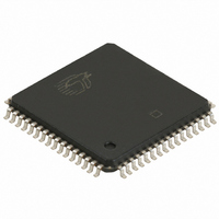
CY7C4841-10AC Cypress Semiconductor Corp, CY7C4841-10AC Datasheet - Page 18

CY7C4841-10AC
Manufacturer Part Number
CY7C4841-10AC
Description
IC SYNC FIFO 4KX9X2 64LQFP
Manufacturer
Cypress Semiconductor Corp
Series
CY7Cr
Datasheet
1.CY7C4811-10AC.pdf
(23 pages)
Specifications of CY7C4841-10AC
Function
Synchronous, Dual Port
Memory Size
72K (4K x 9 x 2)
Data Rate
100MHz
Access Time
8ns
Voltage - Supply
3.3V
Operating Temperature
-40°C ~ 85°C
Mounting Type
Surface Mount
Package / Case
64-LQFP
Density
64Kb
Word Size
9b
Sync/async
Synchronous
Expandable
Yes
Package Type
TQFP
Operating Supply Voltage (typ)
5V
Operating Supply Voltage (min)
4.5V
Operating Supply Voltage (max)
5.5V
Operating Temp Range
0C to 70C
Operating Temperature Classification
Commercial
Mounting
Surface Mount
Pin Count
64
Lead Free Status / RoHS Status
Contains lead / RoHS non-compliant
Other names
428-1259
Available stocks
Company
Part Number
Manufacturer
Quantity
Price
Company:
Part Number:
CY7C4841-10AC
Manufacturer:
CYPRESS
Quantity:
220
Width Expansion Configuration
Word width may be increased simply by connecting the corre-
sponding input control signals of FIFOs A and B. A composite
flag should be created for each of the end-point status flags
EFA and EFB, also FFA and FFB. The partial status flags
PAEA, PAFB, PAFA, PAFB can be detected from any one de-
vice. Figure 3 demonstrates an 18-bit word width using the two
FIFOs contained in one CY7C4801/4811/4821/4831/4841
/4851. Any word width can be attained by adding additional
CY7C4801/4811/4821/4831/4841/4851s.
Document #: 38-06005 Rev. **
WRITE ENABLE 2/LOAD
WRITECLOCK
WRITE ENABLE
Figure 3. Block Diagram of two FIFOs contained in one CY7C4801/4811/4821/4831/4841/4851 configured for an 18-bit
FULL FLAG
D
0
D
17
18
WEN2/LD
WENA
9
9
WCLKA
FFA
FFB
RESET (RSA)
Read Enable 2
RAM ARRAY A
1024 x 9
2048 x 9
4096 x 9
8192 x 9
256 x 9
512 x 9
(RENA2)
EF
width-expansion.
9
WENB2/LDB
WCLKB
WENB1
RCLKA
RENA1
OEA
9
When the CY7C4801/4811/4821/4831/4841/4851 is in a
Width Expansion Configuration, the Read Enable 2 (RENA2
and RENB2) control unputs can be grounded (see Figure 3).
In
(WENA2/LDA,WENB2/LDB) pins are set LOW at Reset so that
the pin operates as a control to load and read the programma-
ble flag offsets.
Read Enable 2 (RENB2)
this
RAM ARRAY B
FF
1024 x 9
2048 x 9
4096 x 9
8192 x 9
256 x 9
512 x 9
configuration,
RESET(RSB)
9
RCLKB
RENB1
EFB
EFA
OEB
CY7C4831/4841/4851
CY7C4801/4811/4821
the
READCLOCK
READ ENABLE
OUTPUT ENABLE
Q
0
Write
Q
17
48X1–17
Enable
EMPTY FLAG
RESET
18
Page 18 of 23
2/Load


