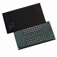
MT48H4M16LFB4-8 Micron Technology Inc, MT48H4M16LFB4-8 Datasheet - Page 8

MT48H4M16LFB4-8
Manufacturer Part Number
MT48H4M16LFB4-8
Description
IC SDRAM 64MBIT 125MHZ 54VFBGA
Manufacturer
Micron Technology Inc
Datasheet
1.MT48H4M16LFB4-10.pdf
(54 pages)
Specifications of MT48H4M16LFB4-8
Format - Memory
RAM
Memory Type
Mobile SDRAM
Memory Size
64M (4M x 16)
Speed
125MHz
Interface
Parallel
Voltage - Supply
1.7 V ~ 1.9 V
Operating Temperature
0°C ~ 70°C
Package / Case
54-VFBGA
Lead Free Status / RoHS Status
Lead free / RoHS Compliant
Available stocks
Company
Part Number
Manufacturer
Quantity
Price
Company:
Part Number:
MT48H4M16LFB4-8
Manufacturer:
Micron Technology Inc
Quantity:
10 000
Part Number:
MT48H4M16LFB4-8
Manufacturer:
MICRON/镁光
Quantity:
20 000
Company:
Part Number:
MT48H4M16LFB4-8 IT
Manufacturer:
Micron Technology Inc
Quantity:
10 000
Company:
Part Number:
MT48H4M16LFB4-8 IT TR
Manufacturer:
Micron Technology Inc
Quantity:
10 000
Company:
Part Number:
MT48H4M16LFB4-8 IT:H
Manufacturer:
Micron Technology Inc
Quantity:
10 000
Company:
Part Number:
MT48H4M16LFB4-8 IT:H TR
Manufacturer:
Micron Technology Inc
Quantity:
10 000
Part Number:
MT48H4M16LFB4-8-IT:H
Manufacturer:
MICRON
Quantity:
20 000
Part Number:
MT48H4M16LFB4-8:H
Manufacturer:
MICRON
Quantity:
20 000
Functional Description
are quad-bank DRAMs that operate at 1.8V and
include a synchronous interface (all signals are regis-
tered on the positive edge of the clock signal, CLK).
Each of the x16’s 16,777,216-bit banks is organized as
4,096 rows by 256 columns by 16 bits.
ented; accesses start at a selected location and con-
tinue for a programmed number of locations in a
programmed sequence. Accesses begin with the regis-
tration of an ACTIVE command, which is then fol-
lowed by a READ or WRITE command. The address
bits registered coincident with the ACTIVE command
are used to select the bank and row to be accessed
(BA0 and BA1 select the bank, A0-A11 select the row).
The address bits (A0–A7) registered coincident with
the READ or WRITE command are used to select the
starting column location for the burst access.
tialized. The following sections provide detailed infor-
mation
definition, command descriptions and device opera-
tion.
Initialization
predefined manner. Operational procedures other
than those specified may result in undefined opera-
tion. Power should be applied to V
taneously. Once the power is applied to V
and the clock is stable (stable clock is defined as a sig-
nal cycling within timing constraints specified for the
clock pin), the SDRAM requires a 100µs delay prior to
issuing any command other than a COMMAND
INHIBIT or NOP. Starting at some point during this
100µs period and continuing at least through the end
of this period, command inhibit or NOP commands
should be applied.
one command inhibit or NOP command having been
applied, a PRECHARGE command should be applied.
All banks must then be precharged, thereby placing
the device in the all banks idle state.
be performed. After the AUTO refresh cycles are com-
plete, the SDRAM is ready for mode register program-
ming. Because the mode register will power up in an
unknown state, it should be loaded prior to applying
any operational command.
pdf: 09005aef80a63953, source: 09005aef808a7edc
Y25L_64Mb_2.fm - Rev. E 11/04 EN
In general, the 64Mb SDRAMs (1 Meg x 16 x 4 banks)
Read and write accesses to the SDRAM are burst ori-
Prior to normal operation, the SDRAM must be ini-
SDRAMs must be powered up and initialized in a
Once the 100µs delay has been satisfied with at least
Once in the idle state, two AUTO refresh cycles must
covering
device
initialization,
DD
and V
DD
DD
and V
Q simul-
register
DD
Q
8
Mode Register Definition
are two mode registers in the mobile component,
mode register and extended mode register. The mode
register is illustrated in Figure 4, Mode Register Defini-
tion, on page 9 (the extended mode register is illus-
trated in Figure 6, Extended Mode Register Table, on
page 11).
operation of the SDRAM, including burst length, burst
type, CAS latency, operating mode and write burst
mode. The mode register is programmed via the LOAD
MODE REGISTER command and will retain the stored
information until it is programmed again or the device
loses power.
M3 specifies the type of burst (sequential or inter-
leaved), M4–M6 specify the CAS latency, M7 and M8
specify the operating mode, M9 specifies the write
burst mode, and M10, and M11 should be set to zero.
M12 and M13 should be set to zero to prevent
extended mode register.
are idle, and the controller must wait the specified
time before initiating the subsequent operation. Vio-
lating either of these requirements will result in
unspecified operation.
Burst Length
ented, with the burst length being programmable, as
shown in Figure 4, Mode Register Definition, on
page 9. The burst length determines the maximum
number of column locations that can be accessed for a
given READ or WRITE command. Burst lengths of 1, 2,
4, or 8 locations are available for both the sequential
and the interleaved burst types, and a full-page burst is
available for the sequential type. The full-page burst is
used in conjunction with the BURST TERMINATE
command to generate arbitrary burst lengths.
operation or incompatibility with future versions may
result.
of columns equal to the burst length is effectively
selected. All accesses for that burst take place within
this block, meaning that the burst will wrap within the
block if a boundary is reached. The block is uniquely
selected by A0–A7 when the burst length is set to two;
by A2–A7 when the burst length is set to four; and by
A3–A7 when the burst length is set to eight.
In order to achieve low power consumption, there
The mode register defines the specific mode of
Mode register bits M0–M2 specify the burst length,
The mode register must be loaded when all banks
Read and write accesses to the SDRAM are burst ori-
Reserved states should not be used, as unknown
When a READ or WRITE command is issued, a block
Micron Technology, Inc., reserves the right to change products or specifications without notice.
MOBILE SDRAM
©2003 Micron Technology, Inc. All rights reserved.
64Mb: x16


