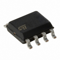
M93S66-WMN6P STMicroelectronics, M93S66-WMN6P Datasheet - Page 9

M93S66-WMN6P
Manufacturer Part Number
M93S66-WMN6P
Description
IC EEPROM 4KBIT 2MHZ 8SOIC
Manufacturer
STMicroelectronics
Specifications of M93S66-WMN6P
Format - Memory
EEPROMs - Serial
Memory Type
EEPROM
Memory Size
4K (256 x 16)
Speed
2MHz
Interface
Microwire, 3-Wire Serial
Voltage - Supply
2.5 V ~ 5.5 V
Operating Temperature
-40°C ~ 85°C
Package / Case
8-SOIC (3.9mm Width)
Organization
256 K x 16
Interface Type
Microwire
Maximum Clock Frequency
2 MHz
Supply Voltage (max)
5.5 V
Supply Voltage (min)
2.5 V
Maximum Operating Current
2 mA
Maximum Operating Temperature
+ 85 C
Mounting Style
SMD/SMT
Minimum Operating Temperature
- 40 C
Operating Supply Voltage
2.5 V, 5.5 V
Capacitance, Input
5 pF
Capacitance, Output
5 pF
Current, Input, Leakage
±2.5 μA
Current, Operating
2 mA
Current, Output, Leakage
±2.5
Current, Supply
1.5⁄2.0 mA
Data Retention
>40 yrs.
Density
4K
Package Type
SO8
Temperature, Operating
-40 to +85 °C
Temperature, Operating, Maximum
85 °C
Temperature, Operating, Minimum
-40 °C
Time, Address Setup
50
Time, Fall
50 ns
Time, Rise
50 ns
Voltage, Esd
4000 V
Voltage, Input, High
3.5 to 6.5 V
Voltage, Input, High Level
0.7 V
Voltage, Input, Low
0.5 to 1.1 V
Voltage, Input, Low Level
–0.45 V
Voltage, Output, High
6 to 13.2 V
Voltage, Output, Low
0.4 V
Voltage, Supply
2.5 to 5.5 V
Lead Free Status / RoHS Status
Lead free / RoHS Compliant
Other names
497-8598-5
M93S66-WMN6P
M93S66-WMN6P
Read
The Read Data from Memory (READ) instruction
outputs serial data on Serial Data Output (Q).
When the instruction is received, the op-code and
address are decoded, and the data from the mem-
ory is transferred to an output shift register. A dum-
my 0 bit is output first, followed by the 16-bit word,
with the most significant bit first. Output data
changes are triggered by the rising edge of Serial
Clock (C). The M93Sx6 automatically increments
the internal address register and clocks out the
next byte (or word) as long as the Chip Select In-
put (S) is held High. In this case, the dummy 0 bit
is not output between bytes (or words) and a con-
tinuous stream of data can be read.
Write Enable and Write Disable
The Write Enable (WEN) instruction enables the
future execution of write instructions, and the Write
Disable (WDS) instruction disables it. When power
is first applied, the M93Sx6 initializes itself so that
write instructions are disabled. After an Write En-
able (WEN) instruction has been executed, writing
remains enabled until an Write Disable (WDS) in-
struction is executed, or until V
power-on reset threshold voltage. To protect the
memory contents from accidental corruption, it is
advisable to issue the Write Disable (WDS) in-
struction after every write cycle. The Read Data
from Memory (READ) instruction is not affected by
the Write Enable (WEN) or Write Disable (WDS)
instructions.
CC
falls below the
Write
The Write Data to Memory (WRITE) instruction is
composed of the Start bit plus the op-code fol-
lowed by the address and the 16 data bits to be
written.
Write Enable (W) must be held High before and
during the instruction. Input address and data, on
Serial Data Input (D) are sampled on the rising
edge of Serial Clock (C).
After the last data bit has been sampled, the Chip
Select Input (S) must be taken Low before the next
rising edge of Serial Clock (C). If Chip Select Input
(S) is brought Low before or after this specific time
frame, the self-timed programming cycle will not
be started, and the addressed location will not be
programmed.
While the M93Sx6 is performing a write cycle, but
after a delay (t
becomes available, Chip Select Input (S) can be
driven High to monitor the status of the write cycle:
Serial Data Output (Q) is driven Low while the
M93Sx6 is still busy, and High when the cycle is
complete, and the M93Sx6 is ready to receive a
new instruction. The M93Sx6 ignores any data on
the bus while it is busy on a write cycle. Once the
M93Sx6 is Ready, Serial Data Output (Q) is driven
High, and remains in this state until a new start bit
is decoded or the Chip Select Input (S) is brought
Low.
Programming is internally self-timed, so the exter-
nal Serial Clock (C) may be disconnected or left
running after the start of a write cycle.
SLSH
M93S66, M93S56, M93S46
) before the status information
9/34


