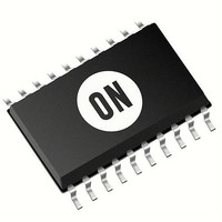
NCP1081DER2G ON Semiconductor, NCP1081DER2G Datasheet - Page 13

NCP1081DER2G
Manufacturer Part Number
NCP1081DER2G
Description
IC CONV CTLR POE-PD 40W 20-TSSOP
Manufacturer
ON Semiconductor
Type
Power over Ethernet Switch (PoE)r
Datasheet
1.NCP1081DER2G.pdf
(17 pages)
Specifications of NCP1081DER2G
Applications
Remote Peripherals (Industrial Controls, Cameras, Data Access)
Internal Switch(s)
Yes
Current Limit
1.1A
Voltage - Supply
0 V ~ 57 V
Operating Temperature
-40°C ~ 85°C
Mounting Type
Surface Mount
Package / Case
20-TSSOP Exposed Pad, 20-eTSSOP, 20-HTSSOP
Output Voltage
9 V
Switching Frequency
250 KHz
Maximum Operating Temperature
+ 85 C
Mounting Style
SMD/SMT
Minimum Operating Temperature
- 40 C
Operating Temperature Range
- 40 C to + 85 C
Output Power
40 W
Input Voltage
57V
Supply Current
510mA
Digital Ic Case Style
TSSOP
No. Of Pins
20
Duty Cycle (%)
80%
Uvlo
38V
Frequency
500kHz
Svhc
No SVHC (20-Jun-2011)
Rohs Compliant
Yes
Lead Free Status / RoHS Status
Lead free / RoHS Compliant
Available stocks
Company
Part Number
Manufacturer
Quantity
Price
Company:
Part Number:
NCP1081DER2G
Manufacturer:
IXYS
Quantity:
7 710
converter and completes initialization, the microprocessor
should check if the NCP1081 detected a two event hardware
classification by reading its digital input (pin IN1 in this
example). If pin IN1 is low, the application knows power is
supplied by a draft IEEE802.3at (D3.0) compliant PSE, and
can deliver power up to the level specified by the draft
IEEE802.3at (D3.0) standard.
classification with the PSE. There are several scenarios for
which the NCP1081 will not enable its nCLASS_AT pin:
•
•
•
Power Mode
PSE and PD devices move into the operating mode.
Under Voltage Lock Out (UVLO)
(ULVO) circuit which monitors the input voltage and
determines when to apply power to the DC−DC controller.
UVLO must be connected to VPORTN
signature resistor has to be placed directly between
VPORTP and VPORTN
As soon as the application is powered by the DC−DC
Otherwise the application will have to perform a Layer 2
When the classification hand−shake is completed, the
The NCP1081 incorporates an under voltage lock out
To use the default settings for UVLO (see Table 3), the pin
The PSE skipped the classification phase.
The PSE performed a one event hardware classification
(it can be a IEEE 802.3af or a draft IEEE802.3at (D3.0)
compliant PSE with Layer 2 engine).
The PSE performed a two event hardware classification
but it did not properly control the input voltage in the
mark voltage window, (for example it crossed the reset
range).
VPORT
Figure 9. Default UVLO Settings
Rdet
1,2
, as shown in Figure 9.
UVLO
VPORTN1,2
VPORTP
NCP1081
1,2
. In this case the
http://onsemi.com
13
must be connected to the center of an external resistor
divider between VPORTP and VPORTN
Figure 10. The series resistance value of the external
resistors must add to 25.5 kW and replaces the internal
signature resistor.
R2 can be calculated using the following equations:
has an external reference voltage hysteresis of 15 percent
typical.
Inrush and Operational Current Limitations
are programmed individually by an external Rinrush and
Rilim1 resistors respectively connected between INRUSH
and VPORTN
shown in Figure 11.
To define the UVLO threshold externally, the UVLO pin
For a Vuvlo_on desired turn−on voltage threshold, R1 and
When using the external resistor divider, the NCP1081
The inrush current limit and the operational current limit
VPORT
Figure 10. External UVLO Configuration
1,2
R1
R2
, and between ILIM1 and VPORTN
R1 ) R2 + R
R2 +
V
ulvo_on
1.2
UVLO
VPORTN1,2
VPORTP
det
R
det
NCP1081
1,2
as shown in
1,2
as


