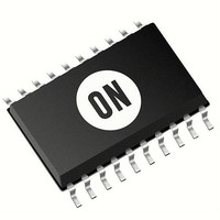
NCP1081DER2G ON Semiconductor, NCP1081DER2G Datasheet - Page 6

NCP1081DER2G
Manufacturer Part Number
NCP1081DER2G
Description
IC CONV CTLR POE-PD 40W 20-TSSOP
Manufacturer
ON Semiconductor
Type
Power over Ethernet Switch (PoE)r
Datasheet
1.NCP1081DER2G.pdf
(17 pages)
Specifications of NCP1081DER2G
Applications
Remote Peripherals (Industrial Controls, Cameras, Data Access)
Internal Switch(s)
Yes
Current Limit
1.1A
Voltage - Supply
0 V ~ 57 V
Operating Temperature
-40°C ~ 85°C
Mounting Type
Surface Mount
Package / Case
20-TSSOP Exposed Pad, 20-eTSSOP, 20-HTSSOP
Output Voltage
9 V
Switching Frequency
250 KHz
Maximum Operating Temperature
+ 85 C
Mounting Style
SMD/SMT
Minimum Operating Temperature
- 40 C
Operating Temperature Range
- 40 C to + 85 C
Output Power
40 W
Input Voltage
57V
Supply Current
510mA
Digital Ic Case Style
TSSOP
No. Of Pins
20
Duty Cycle (%)
80%
Uvlo
38V
Frequency
500kHz
Svhc
No SVHC (20-Jun-2011)
Rohs Compliant
Yes
Lead Free Status / RoHS Status
Lead free / RoHS Compliant
Available stocks
Company
Part Number
Manufacturer
Quantity
Price
Company:
Part Number:
NCP1081DER2G
Manufacturer:
IXYS
Quantity:
7 710
Stresses exceeding Maximum Ratings may damage the device. Maximum Ratings are stress ratings only. Functional operation above the
Recommended Operating Conditions is not implied. Extended exposure to stresses above the Recommended Operating Conditions may affect
device reliability.
1. Tj−TSD allowed during error conditions only. It is assumed that this maximum temperature condition does not occur more than 1 hour
2. Mounted on a 1S2P (3 layer) test board with copper coverage of 25 percent for the signal layers and 90 percent copper coverage for the
3. Surges per EN61000−4−2, 1999 applied between RJ−45 and output ground and between adapter input and output ground of the evaluation
Table 2. Absolute Maximum Ratings
nCLASS_AT
ESD−HBM
ESD−CDM
ESD−SYS
cumulative during the useful life for reliability reasons.
inner planes at an ambient temperature of 85°C in still air. Refer to JEDEC JESD51−7 for details.
board. The specified values are the test levels and not the failure levels.
ESD−MM
VPORTP
INRUSH
Symbol
CLASS
Tj−TSD
TEST1
TEST2
COMP
ARTN
VDDH
UVLO
VDDL
ILIM1
OSC
RTN
T
T
CS
SS
FB
LU
Ta
Tj
θJA
stg
Human Body Model
Charged Device Model
Machine Model
Latch−up
System ESD (contact/air) (Note 3)
Input power supply
Analog ground supply 2
Internal regulator output
Internal regulator output
Analog output
Analog output
Analog output
Analog input
Analog output
Analog input / output
Analog input
Analog input
Analog input
Analog output
Digital inputs
Ambient temperature
Junction temperature
Junction temperature (Note 1)
Storage Temperature
Thermal Resistance,
Junction to Air (Note 2)
Parameter
±200
Min.
−0.3
−0.3
−0.3
−0.3
−0.3
−0.3
−0.3
−0.3
−0.3
−0.3
−0.3
−0.3
−0.3
−0.3
−0.3
8/15
−40
−55
750
300
3.5
−
−
http://onsemi.com
Max.
37.6
150
175
150
3.6
3.6
3.6
3.6
3.6
3.6
3.6
3.6
3.6
3.6
3.6
3.6
72
72
17
85
−
−
−
−
−
6
Units
°C/W
mA
kV
kV
°C
°C
°C
°C
V
V
V
V
V
V
V
V
V
V
V
V
V
V
V
V
V
per MIL−STD−883, Method 3015
per JEDEC Standard JESD78
Voltage with respect to VPORTN
Pass−switch in off−state
(Voltage with respect to VPORTN
Voltage with respect to ARTN
Voltage with respect to ARTN
Voltage with respect to VPORTN
Voltage with respect to VPORTN
Voltage with respect to VPORTN
Voltage with respect to VPORTN
Voltage with respect to ARTN
Voltage with respect to ARTN
Voltage with respect to ARTN
Voltage with respect to ARTN
Voltage with respect to ARTN
Voltage with respect to ARTN
Voltage with respect to VPORTN
Thermal shutdown condition
Exposed pad connected to VPORTN
Conditions
1,2
1,2
1,2
1,2
1,2
1,2
1,2
)
1,2
ground


