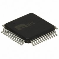
MIC2592B-2BTQ Micrel Inc, MIC2592B-2BTQ Datasheet - Page 18

MIC2592B-2BTQ
Manufacturer Part Number
MIC2592B-2BTQ
Description
IC CTRLR HOTPLUG PCI DUAL 48TQFP
Manufacturer
Micrel Inc
Type
Hot-Swap Controllerr
Datasheet
1.MIC2592B-2YTQ.pdf
(31 pages)
Specifications of MIC2592B-2BTQ
Applications
General Purpose, PCI Express
Internal Switch(s)
No
Voltage - Supply
3.3V, 12V
Operating Temperature
0°C ~ 70°C
Mounting Type
Surface Mount
Package / Case
48-TQFP
Lead Free Status / RoHS Status
Contains lead / RoHS non-compliant
Available stocks
Company
Part Number
Manufacturer
Quantity
Price
outputs are independent of the MAIN outputs (12VIN[A/B]
and 3VIN[A/B]). Should the MAIN supply inputs move
below their respective UVLO thresholds, VAUX[A/B] will
still function as long as VSTBY[A/B] is present. Prior to
standby mode, ONA and ONB (or the Control Registers'
MAINA and MAINB bits) inputs should be deasserted or
the MIC2592B will assert /FAULT[A/B] and /INT (if inter-
rupts are enabled) output signals, if an undervoltage condi-
tion on the MAIN supply inputs is detected.
Circuit Breaker Function
The MIC2592B provides an electronic circuit breaker func-
tion that protects against excessive loads, such as short
circuits, at each supply. When the current from one or more
of a slot’s MAIN outputs exceeds the current limit threshold
(I
circuit breaker is tripped and both MAIN supplies (all outputs
except VAUX[A/B]) are shut off. Should the load current cause
a MAIN output’s V
immediately shut off with no delay. Undervoltage conditions
on the MAIN supply inputs also trip the circuit breaker, but
only when the MAIN outputs are enabled (to signal a supply
input brown-out condition).
The VAUX[A/B] outputs have a different circuit-breaker func-
tion. The VAUX[A/B] circuit breakers do not incorporate a
fast-trip detector, instead they regulate the output current into
a fault to avoid exceeding their operating current limit. The
circuit breaker will trip due to an overcurrent on VAUX[A/B]
when the fault timer expires. This use of the t
vents the circuit breaker from tripping prematurely due to
brief current transients.
Following a fault condition, the outputs can be turned on
again via the ON inputs (if the fault occurred on one of the
MAIN outputs), via the AUXEN inputs (if the fault occurred
on the AUX outputs), or by cycling both ON and AUXEN (if
faults occurred on both the MAIN and AUX outputs). A fault
condition can alternatively be cleared under SMI control of
the ENABLE bits in the CNTRL[A/B] registers (see Register
Bits D[1:0]). When the circuit breaker trips, /FAULT[A/B] will
March 2005
LIM
= 50mV/R
12VOUT_UV[A/B]
FORCE_ON[A/B]
FORCE_EN[A/B]
3VOUT_UV[A/B]
3VAUX_UV[A/B]
SENSE
SENSE
AUXEN[A/B]
VAUX[A/B]
MAIN[A/B]
(1)
(2)
(3)
(4)
(5)
) for a duration greater than t
ON[A/B]
External pin
CNTRL[A/B] Register Bit D[0]
Internal flag
CNTRL[A/B] Register Bit D[1]
CNTRL[A/B] Register Bit D[2]
to exceed V
(1)
(2)
(3)
(1)
(4)
(3)
(3)
(1)
(5)
THFAST
THFAST
THFAST
Figure 8. /PWRGD[A/B] Logic Diagram
, the outputs are
, the outputs are
FLT
FLT
FLT
timer pre-
timer pre-
FLT
FLT
FLT
, the
, the
18
be asserted if the outputs were enabled through the Hot-Plug
Interface inputs. At the same time, /INT will be asserted (un-
less interrupts are masked). Note that /INT is deasserted by
writing a Logic 1 back into the respective fault bit position(s)
in the STAT[A/B] register or the Common Status Register.
The response time (t
rent detector is set by external capacitors at the CFILTER[A/B]
pins to GND. For Slot A, CFILTER[A] is located at Pin 2; for
Slot B, CFILTER[B] is located at Pin 35. For a given response
time, the value for C
where t
I
cal Characteristics” table.
For applications that require a more accurate response
time for a given C
employs a patent-pending technique that improves re-
employs a patent-pending technique that improves re-
sponse time accuracy by more than a factor of two. A
110kΩ, 1% resistor connected from the MIC2592B’s
RFILTER[A&B] pin (Pin 20) to GND can be used. In this
case, the value for C
(t
is 110kΩ, and “SF” is the CFILTER[A/B] response time
“Scaling Factor” in the “Electrical Characteristics” table.
FILTER
where t
FLT
) is given by:
C
C
and V
and V
FLT[A/B]
FLT[A/B]
FLT[A/B]
FILTER[A /B]
FILTER[A /B]
FLT
, and “SF” is the CFILTER[A/B] response time
FILTER
is the desired response time, R
is the desired response time and quantities
are specifi ed in the MIC2592B’s “Electri-
F
F
FLT
FILTER[A/B]
V
FILTER[A/B]
FILTER[A/B]
FILTER[A/B]
FILTER[A/B]
STBY
) of the MIC2592B’s primary overcur-
R
t
4.99 k
FLT A B
FILTER[A&B]
V
FILTER
t
FLT
/PWRGD[A/B]
is given by:
for a desired response time
ms
tolerance, the MIC2592B
ms
k
V
I
FILTER
10
SF
3
A
M9999-033105
FILTER[A&B]
FILTER[A&B]
FILTER[A&B]


