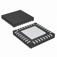
MAX16816ATJ+T Maxim Integrated Products, MAX16816ATJ+T Datasheet - Page 18

MAX16816ATJ+T
Manufacturer Part Number
MAX16816ATJ+T
Description
IC LED DRIVR HIGH BRIGHT 32-TQFN
Manufacturer
Maxim Integrated Products
Type
HBLED Driverr
Datasheet
1.MAX16816ATJ.pdf
(33 pages)
Specifications of MAX16816ATJ+T
Topology
PWM, SEPIC, Step-Down (Buck), Step-Up (Boost)
Number Of Outputs
1
Internal Driver
Yes
Type - Primary
Automotive
Type - Secondary
High Brightness LED (HBLED)
Frequency
125kHz ~ 500kHz
Voltage - Supply
5.5 V ~ 76 V
Mounting Type
Surface Mount
Package / Case
32-TQFN Exposed Pad
Operating Temperature
-40°C ~ 125°C
Internal Switch(s)
Yes
Efficiency
90%
Low Level Output Current
76 mA
High Level Output Current
67 mA
Operating Supply Voltage
5.5 V to 76 V
Maximum Supply Current
4.5 mA
Maximum Power Dissipation
2758 mW
Maximum Operating Temperature
+ 125 C
Mounting Style
SMD/SMT
Minimum Operating Temperature
- 40 C
Lead Free Status / RoHS Status
Lead free / RoHS Compliant
Voltage - Output
-
Current - Output / Channel
-
Lead Free Status / Rohs Status
Details
where V
age between SNS+ and SNS- and I
inductor current at full load and minimum input voltage.
When the voltage drop across R
ILIM threshold, the MOSFET driver (DRV) terminates
the on-cycle and turns the switch off, reducing the cur-
rent through the inductor. The FET is turned back on at
the beginning of the next switching cycle.
When the voltage across R
(typ) HICCUP threshold, the HIC comparator terminates
the on-cycle of the device, turning the switching MOS-
FET off. Following a startup delay of 8ms (typ), the
MAX16816 reinitiates soft-start. The device will continue
to operate in HICCUP mode until the overcurrent condi-
tion is removed.
A programmable built-in leading-edge blanking circuit
of the current-sense signal prevents these comparators
from prematurely terminating the on-cycle of the exter-
nal switching MOSFET (Q
from 75ns to 150ns by configuring the Blanking Time
register in the EEPROM. In some cases, the maximum
blanking time may not be adequate and an additional
RC filter may be required to prevent spurious turn-off.
The load sense resistor, R
through the LEDs. The internal floating current-sense
amplifier, CSA, measures the differential voltage across
R
current through R
referred to AGND. The closed-loop regulates the load
current to a value, I
where V
of V
between 100mV and 166mV. See the EEPROM and
Programming section for more information on adjusting
the binning voltage.
The amount of slope compensation required is largely
dependent on the down-slope of the inductor current
when the switching MOSFET, Q
down-slope depends on the input-to-output voltage dif-
ferential of the converter, the inductor value, and the
switching frequency. For stability, the compensation
slope should be equal to or greater than half of the
inductor current down-slope multiplied by the current-
sense resistance (R
Programmable Switch-Mode LED Driver
with Analog-Controlled PWM Dimming
18
CS
SS
, and generates a voltage proportional to the load
______________________________________________________________________________________
in the Binning Adjustment register in the EEPROM
SS
SENSE
is the binning adjustment voltage. Set the value
is the 200mV maximum differential volt-
LED
I
SENSE
CS
LED
, given by the following equation:
at CS. This voltage on CS is
= V
).
S
SS
SENSE
). Select a blanking time
Slope Compensation
CS
Load Current Sense
/ R
, monitors the current
S
CS
, is off. The inductor
SENSE
exceeds the 300mV
PEAK
exceeds the
is the peak
See the EEPROM and Programming section for more infor-
mation on the ESLP register.
The MAX16816 includes a built-in voltage amplifier,
with three-state output, which can be used to close the
feedback loop. The buffered output current-sense sig-
nal appears at CS, which is connected to the inverting
input, FB, of the error amplifier through resistor R
noninverting input is connected to an internally trimmed
current reference.
The output of the error amplifier is controlled by the signal
applied to DIM. When DIM is high, the output of the ampli-
fier is connected to COMP. The amplifier output is open
when DIM is low. This enables the integrating capacitor to
hold the charge when the DIM signal has turned off the
gate drive. When DIM is high again, the voltage on the
compensation capacitors, C
into steady state almost instantaneously.
PWM dimming is achieved by driving DIM with either a
PWM signal or a DC signal. The PWM signal is con-
nected internally to the error amplifier, the dimming
MOSFET gate driver, and the switching MOSFET gate
driver. When the DIM signal is high, the dimming MOSFET
and the switching MOSFET drivers are enabled and the
output of the voltage-error amplifier is connected to
the external compensation network. Also, the buffered
current-sense signal is connected to CS. Preventing
discharge of the compensation capacitor when the
DIM signal is low allows the control loop to return the
LED current to its original value almost instantaneously.
When the DIM signal goes low, the output of the error
amplifier is disconnected from the compensation net-
work and the compensation capacitors, C
voltage is preserved. Choose low-leakage capacitors
for C
switching MOSFETs are disabled, and the converter
stops switching. The inductor energy is now transferred
to the output capacitors.
When the DIM signal goes high and the gate drivers
are enabled, the additional voltage on the output
capacitor may cause a current spike on the LED string.
A larger output capacitor will result in a smaller current
spike. If the overcurrent spike exceeds 30% of the pro-
grammed LED current, the dimming is turned off and
the MAX16816 reinitiates soft-start.
Internal Voltage-Error Amplifier (EAMP)
1
and C
2
. The drivers for the external dimming and
1
and C
2
, forces the converter
PWM Dimming
1
and C
1
. The
2
,


