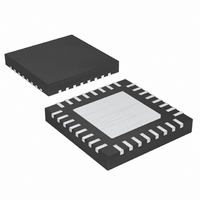
MAX16816ATJ+T Maxim Integrated Products, MAX16816ATJ+T Datasheet - Page 4

MAX16816ATJ+T
Manufacturer Part Number
MAX16816ATJ+T
Description
IC LED DRIVR HIGH BRIGHT 32-TQFN
Manufacturer
Maxim Integrated Products
Type
HBLED Driverr
Datasheet
1.MAX16816ATJ.pdf
(33 pages)
Specifications of MAX16816ATJ+T
Topology
PWM, SEPIC, Step-Down (Buck), Step-Up (Boost)
Number Of Outputs
1
Internal Driver
Yes
Type - Primary
Automotive
Type - Secondary
High Brightness LED (HBLED)
Frequency
125kHz ~ 500kHz
Voltage - Supply
5.5 V ~ 76 V
Mounting Type
Surface Mount
Package / Case
32-TQFN Exposed Pad
Operating Temperature
-40°C ~ 125°C
Internal Switch(s)
Yes
Efficiency
90%
Low Level Output Current
76 mA
High Level Output Current
67 mA
Operating Supply Voltage
5.5 V to 76 V
Maximum Supply Current
4.5 mA
Maximum Power Dissipation
2758 mW
Maximum Operating Temperature
+ 125 C
Mounting Style
SMD/SMT
Minimum Operating Temperature
- 40 C
Lead Free Status / RoHS Status
Lead free / RoHS Compliant
Voltage - Output
-
Current - Output / Channel
-
Lead Free Status / Rohs Status
Details
Programmable Switch-Mode LED Driver
with Analog-Controlled PWM Dimming
ELECTRICAL CHARACTERISTICS (continued)
(V
Typical specifications are at T
4
Driver Output Impedance
Peak Sink Current
Peak Source Current
PWM, ILIM, AND HICCUP COMPARATOR
PWM Comparator Offset
Voltage
Peak Current-Limit
Comparator Trip Threshold
Peak Current-Limit
Comparator Propagation
Delay (Excluding Blanking
Time)
HICCUP Comparator Trip
Threshold
SNS+ Input Bias Current
SNS- Input Bias Current
BLANKING TIME
Blanking Time
ERROR AMPLIFIER
FB Input Bias Current
EAMP Output Sink Current
EAMP Output Source Current
EAMP Input Common-Mode
Voltage
EAMP Output Clamp Voltage
Voltage Gain
Unity-Gain Bandwidth
OSCILLATOR, OSC SYNC, CLK, AND CLKOUT
SYNC Frequency Range
RTSYNC Oscillator Frequency
SYNC High-Level Voltage
SYNC Low-Level Voltage
CC
_______________________________________________________________________________________
= V
UVEN
PARAMETER
= 14V, C
REG1
= 1µF, C
A
= +25°C.)
SYMBOL
f
f
Z
Z
SW_MAX
SW_MIN
V
V
GBW
V
OUT_H
OUT_L
I
I
COM
A
SIHL
SILL
REG2
SK
SR
V
= 1µF, C
V
V
V
V
V
50mV overdrive
V
V
Blanking Time Control Register is ‘00’
Blanking Time Control Register is ‘01’
Blanking Time Control Register is ‘10’
Blanking Time Control Register is ‘11’
V
V
V
(Note 5)
R
R
to AGND
RTOF bit set to ‘0’, R
RTOF bit set to ‘0’, R
DRI
DRI
DRI
DRI
COMP
SNS+
SNS+
FB
FB
FB
COMP
COMP
= 1V
= 1.735V, V
= 0.735V, V
= 7.0V, DRV sinking 250mA
= 7.0V, DRV sourcing 250mA
= 7.0V
= 7.0V
CLMP
= 0V, V
= 0V, V
- (V
= 100kΩ to AGND
= 100kΩ to AGND, C
= 0.1µF, R
SNS+
SNS-
SNS-
COMP
COMP
CONDITIONS
-V
SNS-
= 0V
= 0V
T
T
T
= 100kΩ
= 25kΩ
= 1V
= 1V
)
= 25kΩ, T
COMP
A
= 100pF
= T
J
= -40°C to +125°C, unless otherwise noted.
-100
-100
-100
MIN
160
235
500
106
475
2.8
1.3
3
2
0
TYP
200
300
150
125
100
125
500
2.8
5.0
2.5
1.4
0.8
-65
-65
2.0
0.5
40
75
80
7
7
+100
MAX
245
385
125
143
525
1.6
0.4
2.7
4
8
UNITS
MHz
kHz
kHz
mA
mA
mV
mV
µA
µA
nA
dB
ns
ns
Ω
A
A
V
V
V
V
V


