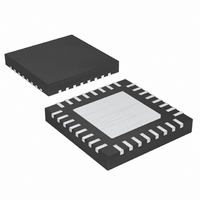
MAX16816ATJ+T Maxim Integrated Products, MAX16816ATJ+T Datasheet - Page 20

MAX16816ATJ+T
Manufacturer Part Number
MAX16816ATJ+T
Description
IC LED DRIVR HIGH BRIGHT 32-TQFN
Manufacturer
Maxim Integrated Products
Type
HBLED Driverr
Datasheet
1.MAX16816ATJ.pdf
(33 pages)
Specifications of MAX16816ATJ+T
Topology
PWM, SEPIC, Step-Down (Buck), Step-Up (Boost)
Number Of Outputs
1
Internal Driver
Yes
Type - Primary
Automotive
Type - Secondary
High Brightness LED (HBLED)
Frequency
125kHz ~ 500kHz
Voltage - Supply
5.5 V ~ 76 V
Mounting Type
Surface Mount
Package / Case
32-TQFN Exposed Pad
Operating Temperature
-40°C ~ 125°C
Internal Switch(s)
Yes
Efficiency
90%
Low Level Output Current
76 mA
High Level Output Current
67 mA
Operating Supply Voltage
5.5 V to 76 V
Maximum Supply Current
4.5 mA
Maximum Power Dissipation
2758 mW
Maximum Operating Temperature
+ 125 C
Mounting Style
SMD/SMT
Minimum Operating Temperature
- 40 C
Lead Free Status / RoHS Status
Lead free / RoHS Compliant
Voltage - Output
-
Current - Output / Channel
-
Lead Free Status / Rohs Status
Details
The MAX16816 uses a feedback loop to control the
load current. The differential voltage across the current-
sense resistor, R
adjustable reference to regulate the LED current. The
voltage across the sense resistor is measured differen-
tially to achieve high immunity to common-mode noise.
The MAX16816 includes a factory-set regulation volt-
age of 133mV ±3% across R
regulation voltage by programming the binning adjust-
ment register (see Table 3). The reference voltage level
may not necessarily be equal to the regulation voltage.
There are offsets involved that are trimmed at the facto-
ry. Read the default register code and step up the code
by one to increase the regulation voltage by 6.66mV.
Step down the code by one to reduce the regulation
voltage by 6.66mV.
REG2 is EEPROM configurable to supply a voltage rang-
ing from 5V to 15V and is capable of sourcing up to
20mA. Connect REG2 to the primary switching MOSFET
gate-driver supply input, DRI, for normal operation.
Table 3. Binning Adjustment Register
Programmable Switch-Mode LED Driver
with Analog-Controlled PWM Dimming
* Not recommended
20
VOLTAGE LEVEL
REFERENCE
______________________________________________________________________________________
173.33*
180.00*
186.67*
193.33*
200.00*
100.00
106.67
113.33
120.00
126.67
133.33
140.00
146.67
153.33
160.00
166.67
(mV)
Binning Adjustment Register (BIN)
CS
, is compared with an internal
REG2 Control Register (DRPS)
27h
0
0
0
0
0
0
0
0
1
1
1
1
1
1
1
1
EEPROM ADDRESS
CS
. Adjust the differential
26h
0
0
0
0
1
1
1
1
0
0
0
0
1
1
1
1
25h
0
0
1
1
0
0
1
1
0
0
1
1
0
0
1
1
24h
0
1
0
1
0
1
0
1
0
1
0
1
0
1
0
1
Adjust REG2 by programming the REG2 Control
Register. See Table 4.
The MAX16816 features a programmable blanking time
to mask out the current-sense signal for a short dura-
tion to avoid the ILIM and HICCUP comparators from
prematurely terminating the on-cycle of the switching
MOSFET. This blanking time allows for higher input cur-
rent during startup without triggering a fault condition.
The blanking time is adjustable in the range of 150ns to
75ns by configuring the EEPROM. See Table 5.
Table 4. REG2 Control Register
Table 5. Blanking Time
* Factory default
* Factory default
BLANKING TIME
REG2 OUTPUT
VOLTAGE
10.333
11.000
11.667
12.333
13.000
13.667
14.333
15.000
7.000*
5.000
5.667
6.333
7.667
8.333
9.000
9.667
150*
(ns)
125
100
Blanking Time Adjustment Register (BLNK)
(V)
75
2Bh
0
0
0
0
0
0
0
0
1
1
1
1
1
1
1
1
33h
0
0
1
1
EEPROM ADDRESS
EEPROM ADDRESS
2Ah
0
0
0
0
1
1
1
1
0
0
0
0
1
1
1
1
29h
0
0
1
1
0
0
1
1
0
0
1
1
0
0
1
1
32h
0
1
0
1
28h
0
1
0
1
0
1
0
1
0
1
0
1
0
1
0
1


