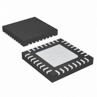
MAX16816ATJ+T Maxim Integrated Products, MAX16816ATJ+T Datasheet - Page 25

MAX16816ATJ+T
Manufacturer Part Number
MAX16816ATJ+T
Description
IC LED DRIVR HIGH BRIGHT 32-TQFN
Manufacturer
Maxim Integrated Products
Type
HBLED Driverr
Datasheet
1.MAX16816ATJ.pdf
(33 pages)
Specifications of MAX16816ATJ+T
Topology
PWM, SEPIC, Step-Down (Buck), Step-Up (Boost)
Number Of Outputs
1
Internal Driver
Yes
Type - Primary
Automotive
Type - Secondary
High Brightness LED (HBLED)
Frequency
125kHz ~ 500kHz
Voltage - Supply
5.5 V ~ 76 V
Mounting Type
Surface Mount
Package / Case
32-TQFN Exposed Pad
Operating Temperature
-40°C ~ 125°C
Internal Switch(s)
Yes
Efficiency
90%
Low Level Output Current
76 mA
High Level Output Current
67 mA
Operating Supply Voltage
5.5 V to 76 V
Maximum Supply Current
4.5 mA
Maximum Power Dissipation
2758 mW
Maximum Operating Temperature
+ 125 C
Mounting Style
SMD/SMT
Minimum Operating Temperature
- 40 C
Lead Free Status / RoHS Status
Lead free / RoHS Compliant
Voltage - Output
-
Current - Output / Channel
-
Lead Free Status / Rohs Status
Details
Table 11. MAX16816 Memory Map (Scratchpad)
sequence begins. All EEPROM bits are copied to the
EEPROM from the scratchpad with a single
SET_WRITE_EE command. This command also sets an
internal BUSY flag to mask all other incoming signals.
SET_WRITE_SCH: The SET_WRITE_SCH command
transfers data to the scratchpad. The 4 MSBs contain the
register address and the 4 LSBs contain the data to be
written. The internal BUSY flag is not set by this com-
mand. Table 11 shows the MAX16816 EEPROM memory
organization. Use the SET_WRITE_EE command to trans-
fer data from the scratchpad to the EEPROM.
SET_READ_SCH: The SET_READ_SCH command is
the command to read data in the scratch pad buffer.
Once the MAX16816 receives the SET_READ_SCH
command, data on the scratchpad register is shifted
out. After 60 clock cycles, the MAX16816 completes
the SET_READ_SCH sequence. The BUSY signal is not
set by this command.
To program the MAX16816 on-chip EEPROM with a
pulldown device, directly connect FAULT to the DATA
IN input of a microcontroller (µC). Also, connect FAULT
to the DATA OUT output of a µC using an external
switch (Figure 5). Connect the EN of the µC directly to
UVEN to control the internal timer of the MAX16816 for
SCRATCHPAD
ADDRESS
6h–9h
Ch
Dh
1h
2h
3h
4h
5h
Ah
Bh
Eh
Fh
______________________________________________________________________________________
Programmable Switch-Mode LED Driver
EEPROM ADDRESS
with Analog-Controlled PWM Dimming
Reserved
Reserved
Reserved
Reserved
Reserved
28h–2Bh
2Ch–2Fh
38h–3Bh
14h–23h
24h–27h
30h–33h
34h–37h
Programming
Reserved
Reserved
Reserved
Reserved
Reserved
Reserved
Binning Adjustment Register
REG2 Control Register
Reserved
Blanking Time Adjustment Register
Digital Soft-Start Duration Register, Internal Oscillator Enable Bit
Slope Compensation Register
programming purposes. Ensure that V
than the UVLO threshold because both UVEN and
FAULT are pulled up to 5V. See the Electrical
Characteristic tables for details.
Figure 5. Programming Through a FAULT Pin
μC
DATA OUT
DATA IN
REGISTER
EN
READ
WRITE
UVEN
FAULT
MAX16816
V
CC
CC
is greater
25


