L9949 STMicroelectronics, L9949 Datasheet
L9949
Specifications of L9949
Available stocks


Related parts for L9949


L9949 Summary of contents
Page 1
... ORDERING NUMBER: L9949 FULL BRIDGE FOR DOOR LATCH OR MIRROR RETRACT, HALF BRIDGES FOR MIRROR AXIS CONTROL AND HIGH-SIDE DRIVER FOR MIRROR DEFROSTER DESCRIPTION The L9949 is a microprocessor controlled power in- terface for automotive applications realized in multipower BCD60III technology three DC mo (battery ...
Page 2
... Standby-Mode The standby mode of the L9949 is activated by setting the bits 12 and 13 of the Input Data Register to zero. All latched data will be cleared and the inputs and outputs are switched to high impedance. In the standby mode ...
Page 3
... DI VS OUT1 GND a temperature warning flag is set and is available via the SPI the thermal shutdown bit will be set and HYS ISC D99AT455Amod L9949 and the thermal shutdown bit ) to dOL = 10µs, the overcurrent flag is set GND OUT6 VCC CSN VS OUT2 GND 3/20 ...
Page 4
... This input is low active and requires CMOS logic levels. The serial data transfer between L9949 and micro controller is enabled by pulling the input CSN to low level input voltage of more than 9.6V above VCC is applied to CSN pin the L9949 will be switched into a test mode. 6 ...
Page 5
... HYS T Thermal Shutdown Threshold jSD ON Junction Temperature T Thermal Shutdown Threshold jSD OFF Junction Temperature T Thermal Shutdown Hysteresis jSD HYS Parameter Parameter Parameter T increasing j T decreasing j T increasing j T decreasing j L9949 Value Unit -0.3... - ±10 A ±5 A Value (1) kV ±2 (2) kV ± ...
Page 6
... L9949 Figure 2. Thermal Data of Package Z (˚C/W) th diss. area dimensions 10 1 0.1 0.001 0.01 ELECTRICAL CHARACTERISTCS 4 GND and currents are assumed positive, when the current flows into the pin Symbol Parameter Supply V Operating Supply Voltage S Range I DC Supply Current S Quiescent Supply Current ...
Page 7
... A OUT1 125 ° 3.0 A OUT1 ° 3.0 A OUT1 ° 3.0 A OUT2 125 ° 3.0 A OUT2 ° 3.0 A OUT2 L9949 . Min. Typ. Max. Unit 7 0 4 --------------- - 10000 1%FS 2%FS 150 m 225 m 180 m 150 m 225 m 180 ...
Page 8
... L9949 ELECTRICAL CHARACTERISTCS (continued 4 GND and currents are assumed positive, when the current flows into the pin Symbol Parameter R On-resistance to Supply or GND ON OUT3 R On-resistance to Supply or GND ON OUT4 R On-resistance to Supply or GND ON OUT5 R On-resistance to Supply ON OUT6 |I | Output Current Limitation to OUT1 Supply or GND ...
Page 9
... Figure 3. TYPICAL R CHARACTERISTICS OUT1,2 ON 160 140 120 100 -40 -20 0 Figure 4. TYPICAL R CHARACTERISTICS OUT3,4,5 ON 1100 1000 900 800 700 600 500 400 300 200 100 0 -40 - TEMP [ TEMP [C] L9949 HS 13. 13 100 120 HS 13. 13 100 120 9/20 ...
Page 10
... L9949 Figure 5. TYPICAL R CHARACTERISTICS OUT6 ON 110 100 -40 -20 0 ELECTRICAL CHARACTERISTCS 4 GND and currents are assumed positive, when the current flows into the pin Symbol Parameter OUTPUTS: OUT1 - OUT6 t Output Delay Time Highside Driver On t Output Delay Time, d OFF H Highside Driver Off ...
Page 11
... VCC CM0 C MOSI MISO *in case of an unexpected freewheeling condition (e.g. POR, TSD or OV event) capacitor value must be high enough to limit maximum Vs voltage of L9949 appl_n_wmf below absolute maximum ratings. = -40 to 150 °C, unless otherwise specified. The voltages are refered to j Test Condition ...
Page 12
... L9949 Figure 7. Functional Block Diagram VS (pin8) HS A-driver LS A-driver OUT1 (pin9) VS (pin8) HS B-driver LS B-driver VS (pin13) HS A-driver LS A-driver OUT2 (pin12) VS (pin13) HS B-driver LS B-driver FUNCTIONAL DESCRIPTION OF THE SPI Serial Peripheral Interface (SPI) This device uses a standard SPI to communicate with a microcontroller. The SPI can be driven by a microcontroller with its SPI peripheral running in either of the two following modes: CPOL = CPHA = 0 or CPOL = CPHA = 1 ...
Page 13
... The input CLK can be tested by clamping the input DI to low level and vice versa. lockout mode. If this bit is set, an over- or undervoltage condition at S lockout bit (bit 14) in the input data register. If bit 14 is cleared, the S returns to normal operating range. In this case no inter- S L9949 13/20 ...
Page 14
... A logical NOR-combination of all bits both status registers. This bit can be polled by the micro-controller without the need of the full SPI communication (see Figure 13). A broken VCC-connection of the L9949 can be detected by the microcontroller, bec ause all 15 bits low or high is not a valid frame. ...
Page 15
... CSN going to high 3.5 V CSN V = 1.5 V CLK < V < 5 -200 25° L9949 . Min. Typ. Max. Unit 200 s 1.5 V 3.5 V 0.5 V -50 -25 -10 µ µ µ 1000 ns 400 ns 400 ns 400 ns 400 ns 200 ns 200 ns 100 ns 100 ns 0.2 0 -1.3 -1 -0.8 15/20 ...
Page 16
... L9949 SPI INTERFACE ELECTRICAL CHARACTERISTCS (continued 4 GND and currents are assumed positive, when the current flows into the pin Symbol Parameter I Tristate Leakage Current DOLK C Tristate Input Capacitance DO DO timing (see Figg. 10 & 11 Rise Time Data Out Fall Time ...
Page 17
... Figure 11. SPI-Interface - Data Out Enable and Disable Time CSN DO pull-up load =100pF L DO pull-down load to GND C =100pF set CSN CLKH set CLK set DI hold DI CLKL Valid Valid tri tri H L9949 50% 0 50% t dis DO L tri 50% t dis DO H tri 17/20 ...
Page 18
... L9949 Figure 12. SPI-Interface - Driver Turn On/Off Timing CSN output current of a driver output current of a driver Figure 13. SPI-Interface - Timing of Status Bit 0 (Fault Condition) CSN high to low and CLK stays low: status information of data bit 0 (fault condition) is transfered to Data Out CSN CLK ...
Page 19
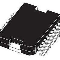
... Weight: 1.9gr 0.021 0.013 0.630 0.386 0.570 0.050 0.450 0.437 0.114 0.244 0.004 0.626 0.043 0.043 0.394 DETAIL B lead a3 11 Gage Plane BOTTOM VIEW E1 10 PSO20MEC L9949 OUTLINE AND JEDEC MO-166 PowerSO20 DETAIL A slug DETAIL B 0. SEATING PLANE (COPLANARITY 0056635 19/20 ...
Page 20
... L9949 Information furnished is believed to be accurate and reliable. However, STMicroelectronics assumes no responsibility for the consequences of use of such information nor for any infringement of patents or other rights of third parties which may result from its use. No license is granted by implication or otherwise under any patent or patent rights of STMicroelectronics. Specifications mentioned in this publication are subject to change without notice ...