L9949 STMicroelectronics, L9949 Datasheet - Page 2
L9949
Manufacturer Part Number
L9949
Description
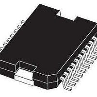
IC DRIVER DOOR ACTUATOR PWRSO-20
Manufacturer
STMicroelectronics
Type
Door Actuator Driverr
Datasheet
1.L9949TR.pdf
(20 pages)
Specifications of L9949
Applications
Automotive
Current - Supply
7mA
Voltage - Supply
7 V ~ 28 V
Operating Temperature
-40°C ~ 150°C
Mounting Type
Surface Mount
Package / Case
PowerSO-20 Exposed Bottom Pad
Product
Half-Bridge Drivers
Supply Current
20 mA
Mounting Style
SMD/SMT
Lead Free Status / RoHS Status
Lead free / RoHS Compliant
Available stocks
Company
Part Number
Manufacturer
Quantity
Price

Part Number:
L9949TR
Manufacturer:
ST
Quantity:
20 000


L9949
DESCRIPTION (continued)
tors and one grounded resistive load can be driven with its three half bridges, one full bridge and one highside
driver power outputs. The integrated standard serial peripheral interface (SPI) controls all operation modes (for-
ward, reverse, brake and high impedance). All diagnostic informations are available via the SPI.
Dual Power Supply: V
The power supply voltage V
charge-pump are used to drive the highside switches. The logic supply voltage V
the logic part and the SPI of the device. Due to the independent logic supply voltage the control and status in-
formation will not be lost, if there are temporary spikes or glitches on the power supply voltage. In case of power-
on (V
power-on-reset (POR). If the voltage V
puts are switched to tristate (high impedance) and the status registers are cleared.
Standby-Mode
The standby mode of the L9949 is activated by setting the bits 12 and 13 of the Input Data Register to zero. All
latched data will be cleared and the inputs and outputs are switched to high impedance. In the standby mode
the current at V
a very low quiescent current can be achieved. If one of the bits 12 and 13 are set to high, the device will be
switched to active mode.
Inductive Loads
Each half bridge is built by internally connected highside and a lowside power DMOS transistor. Due to the built-
in reverse diodes of the output transistors inductive loads can be driven at the outputs OUT1 to OUT5 without
external free-wheeling diodes. The highside driver OUT6 is intended to drive resistive loads only hence only a
limited energie (E<1mJ ) can be dissipated by the internal ESD-diode in freewheeling condition. For inductive
loads (L>100 H) an external free-wheeling diode connected to GND and OUT6 is needed.
Diagnostic Functions
All diagnostic functions (over/open load, power supply over-/undervoltage, temperature warning and thermal
shutdown) are internally filtered and the condition has to be valid for at least 10µs (0.5ms, respectively) before
the corresponding status bit in the status registers will be set. The filters are used to improve the noise immunity
of the device. The open load and temperature warning function are intended for information purpose and will
not change the state of the output drivers. In contrast, the overload and thermal shutdown condition will disable
the corresponding driver (overload) or all drivers (thermal shutdown), respectively. The microcontroller has to
clear the status bits to reactivate the corresponding drivers. This is to avoid an uncontrolled switching behaviour
of the device which may result in a heavy noise on the GND and V
to GND or V
Overvoltage and Undervoltage Detection
If the power supply voltage V
to OUT6 are switched to high impedance state to protect the load. If the supply voltage recovers to normal op-
erating voltage, the device will return to the programmed state (lockout bit 14 = 0). When the voltage V
below the undervoltage threshold V
avoid the operation of the power devices without sufficient gate driving voltage (increased power dissipation). If
the supply voltage V
the programmed state (lockout bit 14 = 0). If the lockout bit 14 is set, the automatic turn-on of the drivers is de-
activated. The microcontroller needs to clear the status bits to reactivate the drivers.
2/20
CC
increases from undervoltage to V
S
).
S
(V
CC
S
) is less than typ. 6µA (40µA) for CSN = high (DO in tristate). By switching the V
and the internal charge-pump recovers to normal operating voltage the system returns to
S
and V
S
S
rises above the overvoltage threshold V
supplies the full bridge, the half bridges and the highside driver. An internal
CC
SUV OFF
CC
decreases under the minimum threshold (V
VCC OFF
(min. 6V), the output stages are switched to high impedance to
= 4.2V) the circuit is initialized by an internally generated
S
lines in case of an fault condition (e.g. short
SOV OFF
(max. 22V), the outputs OUT1
CC
(stabilized 5V) is used for
VCC ON
= 3.4V), the out-
CC
S
voltage
drops
Related parts for L9949
Image
Part Number
Description
Manufacturer
Datasheet
Request
R

Part Number:
Description:
STMicroelectronics [RIPPLE-CARRY BINARY COUNTER/DIVIDERS]
Manufacturer:
STMicroelectronics
Datasheet:
Part Number:
Description:
STMicroelectronics [LIQUID-CRYSTAL DISPLAY DRIVERS]
Manufacturer:
STMicroelectronics
Datasheet:

Part Number:
Description:
BOARD EVAL FOR MEMS SENSORS
Manufacturer:
STMicroelectronics
Datasheet:
Part Number:
Description:
NPN TRANSISTOR POWER MODULE
Manufacturer:
STMicroelectronics
Datasheet:
Part Number:
Description:
TURBOSWITCH ULTRA-FAST HIGH VOLTAGE DIODE
Manufacturer:
STMicroelectronics
Datasheet:
Part Number:
Description:
Manufacturer:
STMicroelectronics
Datasheet:
Part Number:
Description:
DIODE / SCR MODULE
Manufacturer:
STMicroelectronics
Datasheet:
Part Number:
Description:
DIODE / SCR MODULE
Manufacturer:
STMicroelectronics
Datasheet:
Part Number:
Description:
Search -----> STE16N100
Manufacturer:
STMicroelectronics
Datasheet:
Part Number:
Description:
Search ---> STE53NA50
Manufacturer:
STMicroelectronics
Datasheet:
Part Number:
Description:
NPN Transistor Power Module
Manufacturer:
STMicroelectronics
Datasheet:
Part Number:
Description:
DIODE / SCR MODULE
Manufacturer:
STMicroelectronics
Datasheet: