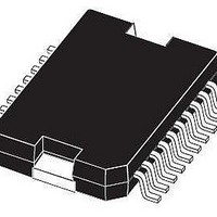
L9949 STMicroelectronics, L9949 Datasheet - Page 12

L9949
Manufacturer Part Number
L9949
Description
IC DRIVER DOOR ACTUATOR PWRSO-20
Manufacturer
STMicroelectronics
Type
Door Actuator Driverr
Datasheet
1.L9949TR.pdf
(20 pages)
Specifications of L9949
Applications
Automotive
Current - Supply
7mA
Voltage - Supply
7 V ~ 28 V
Operating Temperature
-40°C ~ 150°C
Mounting Type
Surface Mount
Package / Case
PowerSO-20 Exposed Bottom Pad
Product
Half-Bridge Drivers
Supply Current
20 mA
Mounting Style
SMD/SMT
Lead Free Status / RoHS Status
Lead free / RoHS Compliant
Available stocks
Company
Part Number
Manufacturer
Quantity
Price
Part Number:
L9949TR
Manufacturer:
ST
Quantity:
20 000
L9949
Figure 7. Functional Block Diagram
FUNCTIONAL DESCRIPTION OF THE SPI
Serial Peripheral Interface (SPI)
This device uses a standard SPI to communicate with a microcontroller. The SPI can be driven by a microcontroller
with its SPI peripheral running in either of the two following modes: CPOL = CPHA = 0 or CPOL = CPHA = 1.
For these two modes, input data is sampled by the low to high transition of the clock CLK, and output data is
changed from the high to low transition of CLK.
The difference of these two modes is the standby polarity of the CLK. For CPOL = 0 the CLK remains low and
for CPOL = 1 the CLK remains high.
This device is not limited to microcontrollers with a build-in SPI. Only three CMOS-compatible output pins and
one input pin will be needed to communicate with the device. A fault condition can be detected by setting CSN
to low. If CSN = 0, the DO-pin will reflect the status bit 0 (fault condition) of the device which is a logical-or of all
bits in the status registers 0 and 1. The microcontroller can poll the status of the device without the need of a
full SPI-communication cycle.
Note: In contrast to the SPI-standard the least significant bit (LSB) will be transfered first (see. FIGURE 8).
Chip Select not (CSN)
The input pin is used to select the serial interface of this device. When CSN is high, the output pin (DO) will be
in high impedance state. A low signal will activate the output driver and a serial communication can be started.
Serial Data In (DI)
The input pin is used to transfer data serial into the device. The data applied to the DI will be sampled at the
12/20
(pin12)
OUT1
(pin9)
OUT2
VS (pin13)
VS (pin13)
VS (pin8)
VS (pin8)
A-driver
A-driver
B-driver
B-driver
A-driver
A-driver
B-driver
B-driver
HS
HS
HS
HS
LS
LS
LS
LS
(pins 1,10,11,20)
GND
Voltage and
Chargepump
Reference
Current
Temperature
DO (pin 17)
Protection
(pin 15)
VCC
CLK (pin 6)
Power-On-Reset
Driver Interface
Current
Monitor
Diagnostic
SPI
(pin 16)
CSN (pin 14)
CM
VCC
DI (pin 7)
(pins 5,8,13,18)
VS
B-driver
A-driver
HS
HS
HS
HS
HS
LS
LS
LS
VS (pin18)
VS (pin18)
VS (pin5)
VS (pin5)
VS (pin5)
ESD
ESD
(pin19)
OUT5
(pin4)
OUT4
(pin3)
OUT3
(pin2)
OUT6


