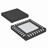
MAX1533ETJ+ Maxim Integrated Products, MAX1533ETJ+ Datasheet - Page 20

MAX1533ETJ+
Manufacturer Part Number
MAX1533ETJ+
Description
IC POWER SUPPLY CONTROLER 32TQFN
Manufacturer
Maxim Integrated Products
Datasheet
1.MAX1533ETJT.pdf
(38 pages)
Specifications of MAX1533ETJ+
Applications
Power Supply Controller
Voltage - Input
4.5 ~ 26 V
Current - Supply
15µA
Operating Temperature
-40°C ~ 85°C
Mounting Type
Surface Mount
Package / Case
32-TQFN Exposed Pad
Product
Power Monitors
Operating Temperature Range
- 40 C to + 85 C
Mounting Style
SMD/SMT
Accuracy
1 %
Sense Voltage (max)
5.5 V
Supply Current (max)
35 uA
Supply Voltage (max)
26 V
Supply Voltage (min)
6 V
Case
QFN
Dc
05+
Lead Free Status / RoHS Status
Lead free / RoHS Compliant
Voltage - Supply
-
Lead Free Status / Rohs Status
Lead free / RoHS Compliant
High-Efficiency, 5x Output, Main Power-Supply
Controllers for Notebook Computers
ON3 and ON5 control SMPS power-up sequencing.
ON3 or ON5 rising above 2.4V enables the respective
outputs. ON3 or ON5 falling below 1.6V disables the
respective outputs. Driving ON_ below 0.8V clears the
overvoltage, undervoltage, and thermal fault latches.
Connecting ON3 or ON5 to REF forces the respective
outputs off while the other output is below regulation
and starts after that output regulates. The second SMPS
remains on until the first SMPS turns off, the device
shuts down, a fault occurs, or LDO5 goes into undervolt-
age lockout. Both supplies begin their power-down
sequence immediately when the first supply turns off.
When output discharge is enabled (OVP pulled low)
and the switching regulators are disabled—by transi-
tions into standby or shutdown mode, or when an
output undervoltage fault occurs—the controller dis-
charges both outputs through internal 12Ω switches,
until the output voltages decrease to 0.3V. This slowly
discharges the output capacitance, providing a soft-
damped shutdown response. This eliminates the slight-
ly negative output voltages caused by quickly
discharging the output through the inductor and low-
side MOSFET. When an SMPS output discharges to
Table 3. Operating Modes
* SHDN is an accurate, low-voltage logic input with 1V falling-edge threshold voltage and 1.6V rising-edge threshold voltage. ON3
and ON5 are 3-level CMOS logic inputs, a logic-low voltage is less than 0.8V, a logic-high voltage is greater than 2.4V, and the mid-
dle logic level is between 1.9V and 2.1V (see the Electrical Characteristics table).
20
Shutdown Mode
Standby Mode
Normal Operation
3.3V SMPS Active
5V SMPS Active
Normal Operation
(Delayed 5V SMPS
Startup)
Normal Operation
(Delayed 3.3V
SMPS Startup)
______________________________________________________________________________________
MODE
SMPS Enable Controls (ON3, ON5)
Output Discharge (Soft-Shutdown)
SHDN
HIGH
HIGH
HIGH
HIGH
HIGH
HIGH
LOW
SMPS Power-Up Sequencing
INPUTS*
HIGH
HIGH
HIGH
ON5
LOW
LOW
REF
X
HIGH
HIGH
HIGH
LOW
LOW
ON3
REF
X
0.3V, its low-side driver (DL_) is forced high, clamping
the respective SMPS output to GND. The reference
remains active to provide an accurate threshold and to
provide overvoltage protection. Both SMPS controllers
contain separate soft-shutdown circuits.
When output discharge is disabled (OVP = V
side drivers (DL_) and high-side drivers (DH_) are both
pulled low, forcing LX into a high-impedance state. Since
the outputs are not actively discharged by the SMPS con-
trollers, the output-voltage discharge rate is determined
only by the output capacitance and load current.
The heart of each current-mode PWM controller is a multi-
input, open-loop comparator that sums two signals: the
output-voltage error signal with respect to the reference
voltage and the slope-compensation ramp (Figure 3).
The MAX1533/MAX1537 use a direct-summing configu-
ration, approaching ideal cycle-to-cycle control over the
output voltage without a traditional error amplifier and the
phase shift associated with it. The MAX1533/MAX1537
use a relatively low loop gain, allowing the use of low-
cost output capacitors. The low loop gain results in the
-0.1% typical load-regulation error and helps reduce
the output capacitor size and cost by shifting the unity-
gain crossover frequency to a lower level.
LDO5
OFF
ON
ON
ON
ON
ON
ON
LDO3
OFF
ON
ON
ON
ON
ON
ON
Fixed-Frequency, Current-Mode
OUTPUTS
3.3V SMPS is in
Power-up after
regulation
5V SMPS
OFF
OFF
OFF
ON
ON
ON
ON
PWM Controller
Power-up after 5V
SMPS is in
regulation
3V SMPS
CC
OFF
OFF
OFF
ON
ON
ON
ON
), the low-


