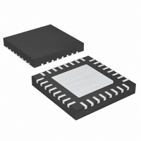
MAX1533ETJ+ Maxim Integrated Products, MAX1533ETJ+ Datasheet - Page 33

MAX1533ETJ+
Manufacturer Part Number
MAX1533ETJ+
Description
IC POWER SUPPLY CONTROLER 32TQFN
Manufacturer
Maxim Integrated Products
Datasheet
1.MAX1533ETJT.pdf
(38 pages)
Specifications of MAX1533ETJ+
Applications
Power Supply Controller
Voltage - Input
4.5 ~ 26 V
Current - Supply
15µA
Operating Temperature
-40°C ~ 85°C
Mounting Type
Surface Mount
Package / Case
32-TQFN Exposed Pad
Product
Power Monitors
Operating Temperature Range
- 40 C to + 85 C
Mounting Style
SMD/SMT
Accuracy
1 %
Sense Voltage (max)
5.5 V
Supply Current (max)
35 uA
Supply Voltage (max)
26 V
Supply Voltage (min)
6 V
Case
QFN
Dc
05+
Lead Free Status / RoHS Status
Lead free / RoHS Compliant
Voltage - Supply
-
Lead Free Status / Rohs Status
Lead free / RoHS Compliant
Switching losses in the high-side MOSFET can become
a heat problem when maximum AC-adapter voltages
are applied, due to the squared term in the switching-
loss equation (C x V
chosen for adequate R
becomes extraordinarily hot when subjected to
V
lower parasitic capacitance.
For the low-side MOSFET (N
dissipation always occurs at maximum battery voltage:
The absolute worst case for MOSFET power dissipation
occurs under heavy-overload conditions that are
greater than I
exceed the current limit and cause the fault latch to trip.
To protect against this possibility, “overdesign” the cir-
cuit to tolerate:
where I
limit circuit, including threshold tolerance and sense-
resistance variation. The MOSFETs must have a
relatively large heatsink to handle the overload power
dissipation.
Choose a Schottky diode (D
drop low enough to prevent the low-side MOSFET’s
body diode from turning on during the dead time. As a
general rule, select a diode with a DC current rating
equal to 1/3rd the load current. This diode is optional
and can be removed if efficiency is not critical.
The boost capacitors (C
enough to handle the gate-charging requirements of
the high-side MOSFETs. Typically, 0.1µF ceramic
capacitors work well for low-power applications driving
medium-sized MOSFETs. However, high-current appli-
cations driving large, high-side MOSFETs require boost
capacitors larger than 0.1µF. For these applications,
select the boost capacitors to avoid discharging the
capacitor more than 200mV while charging the high-
side MOSFETs’ gates:
PD N
IN(MAX)
High-Efficiency, 5x Output, Main Power-Supply
(
L
LIMIT
, consider choosing another MOSFET with
Re
I
LOAD
sistive
is the peak current allowed by the current-
LOAD(MAX)
=
)
______________________________________________________________________________________
=
IN
I
LIMIT
⎡
⎢
⎢
⎣
2
1
x f
DS(ON)
-
BST
⎛
⎜
⎝
SW
but are not high enough to
-
V
Controllers for Notebook Computers
IN MAX
V
). If the high-side MOSFET
⎛
⎜
⎝
) must be selected large
L
L
OUT
(
∆
) with a forward-voltage
), the worst-case power
at low battery voltages
I
INDUCTOR
Boost Capacitors
)
⎞
⎟
⎠
2
⎤
⎥
⎥
⎦
(
I
LOAD
⎞
⎟
⎠
)
2
R
DS ON
(
)
where Q
high-side MOSFET’s data sheet. For example, assume
the FDS6612A n-channel MOSFET is used on the high
side. According to the manufacturer’s data sheet, a sin-
gle FDS6612A has a maximum gate charge of 13nC
(V
boost capacitance is:
Selecting the closest standard value. This example
requires a 0.1µF ceramic capacitor.
The minimum input operating voltage (dropout voltage)
is restricted by the maximum duty-cycle specification
(see the Electrical Characteristics table). However,
keep in mind that the transient performance gets worse
as the step-down regulators approach the dropout volt-
age, so bulk output capacitance must be added (see
the voltage sag and soar equations in the Design
Procedure section). The absolute point of dropout
occurs when the inductor current ramps down during
the off-time (∆I
the on-time (∆I
voltage defined by the following equation:
where V
the charge and discharge paths, respectively. A rea-
sonable minimum value for h is 1.5, while the absolute
minimum input voltage is calculated with h = 1.
The MAX1533/MAX1537 controllers include a minimum
on-time specification, which determines the maximum
input operating voltage that maintains the selected
switching frequency (see the Electrical Characteristics
table). Operation above this maximum input voltage
results in pulse-skipping operation, regardless of the
operating mode selected by SKIP. At the beginning of
each cycle, if the output voltage is still above the feed-
V
IN MIN
GS
(
= 5V). Using the above equation, the required
)
CHG
=
GATE
V
OUT
and V
C
is the total gate charge specified in the
UP
BST
DOWN
Applications Information
+
). This results in a minimum operating
V
DIS
C
=
CHG
BST
) as much as it ramps up during
200
are the parasitic voltage drops in
13
+
=
nC
mV
h
Q
200
⎛
⎜
⎝
GATE
D
Maximum Input Voltage
Minimum Input Voltage
=
MAX
mV
1
Duty-Cycle Limits
0 065µ
.
-
1
⎞
⎟
⎠
F
(
V
OUT
+
V
DIS
33
)


