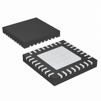
MAX1533ETJ+ Maxim Integrated Products, MAX1533ETJ+ Datasheet - Page 32

MAX1533ETJ+
Manufacturer Part Number
MAX1533ETJ+
Description
IC POWER SUPPLY CONTROLER 32TQFN
Manufacturer
Maxim Integrated Products
Datasheet
1.MAX1533ETJT.pdf
(38 pages)
Specifications of MAX1533ETJ+
Applications
Power Supply Controller
Voltage - Input
4.5 ~ 26 V
Current - Supply
15µA
Operating Temperature
-40°C ~ 85°C
Mounting Type
Surface Mount
Package / Case
32-TQFN Exposed Pad
Product
Power Monitors
Operating Temperature Range
- 40 C to + 85 C
Mounting Style
SMD/SMT
Accuracy
1 %
Sense Voltage (max)
5.5 V
Supply Current (max)
35 uA
Supply Voltage (max)
26 V
Supply Voltage (min)
6 V
Case
QFN
Dc
05+
Lead Free Status / RoHS Status
Lead free / RoHS Compliant
Voltage - Supply
-
Lead Free Status / Rohs Status
Lead free / RoHS Compliant
High-Efficiency, 5x Output, Main Power-Supply
Controllers for Notebook Computers
This offers improved efficiency over a regular 180° out-
of-phase architecture where the duty cycles begin to
overlap below 10V. Figure 10 shows the input-capacitor
RMS current vs. input voltage for an application that
requires 5V/5A and 3.3V/5A. This shows the improve-
ment of the 40/60 optimal interleaving over 50/50 inter-
leaving and in-phase operation.
For most applications, nontantalum chemistries (ceram-
ic, aluminum, or OS-CON) are preferred due to their
resistance to power-up surge currents typical of sys-
tems with a mechanical switch or connector in series
with the input. Choose a capacitor that has less than
10°C temperature rise at the RMS input current for opti-
mal reliability and lifetime.
Most of the following MOSFET guidelines focus on the
challenge of obtaining high load-current capability
when using high-voltage (>20V) AC adapters. Low-cur-
rent applications usually require less attention.
The high-side MOSFET (N
the resistive losses plus the switching losses at both
V
should be roughly equal to the losses at V
lower losses in between. If the losses at V
Figure 10. Input RMS Current
32
IN(MIN)
I
RMS
______________________________________________________________________________________
=
INPUT RMS CURRENT FOR INTERLEAVED OPERATION
INPUT RMS CURRENT FOR SINGLE-PHASE OPERATION
and V
(I
(I
D
I
OUT5
OUT5
RMS
LX5
5.0
4.5
4.0
3.5
3.0
2.5
2.0
1.5
1.0
0.5
0
=
= I
- I
+ I
V
LOAD
6
IN
V
OUT3
OUT5
IN
IN(MAX)
)
2
50/50 INTERLEAVING
(D
INPUT CAPACITOR RMS CURRENT
(
- I
LX5
V
IN
8
OUT
)2 D
D
- D
LX3
(V
OL
OL
V
vs. INPUT VOLTAGE
=
IN
Power-MOSFET Selection
10
) + (I
IN
. Ideally, the losses at V
+ I
V
- V
V
OUT3
IN 2
IN
OUT
OUT3
IN PHASE
(1 - D
H
40/60 OPTIMAL
INTERLEAVING
12
)
V
) must be able to dissipate
- I
IN
)
IN
LX5
D
(V)
)
OL
2
14
(D
- D
= DUTY-CYCLE OVERLAP FRACTION
5V/5A AND 3.3V/5A
LX3
LX3
- D
+ D
16
OL
OL
) +
)
18
IN(MAX)
20
IN(MIN)
IN(MIN)
, with
are
significantly higher, consider increasing the size of N
Conversely, if the losses at V
higher, consider reducing the size of N
not vary over a wide range, maximum efficiency is
achieved by selecting a high-side MOSFET (N
has conduction losses equal to the switching losses.
Choose a low-side MOSFET (N
possible on-resistance (R
ate-sized package (i.e., SO-8, DPAK, or D
reasonably priced. Ensure that the MAX1533/MAX1537
DL_ gate driver can supply sufficient current to support
the gate charge and the current injected into the para-
sitic drain-to-gate capacitor caused by the high-side
MOSFET turning on; otherwise, cross-conduction prob-
lems may occur. Switching losses are not an issue for
the low-side MOSFET since it is a zero-voltage
switched device when used in the step-down topology.
Worst-case conduction losses occur at the duty factor
extremes. For the high-side MOSFET (N
case power dissipation due to resistance occurs at
minimum input voltage:
Generally, use a small high-side MOSFET to reduce
switching losses at high input voltages. However, the
R
pation limits often limits how small the MOSFET can be.
The optimum occurs when the switching losses equal
the conduction (R
losses do not become an issue until the input is greater
than approximately 15V.
Calculating the power dissipation in high-side
MOSFETs (N
it must allow for difficult-to-quantify factors that influ-
ence the turn-on and turn-off times. These factors
include the internal gate resistance, gate charge,
threshold voltage, source inductance, and PC board
layout characteristics. The following switching loss cal-
culation provides only a very rough estimate and is no
substitute for breadboard evaluation, preferably includ-
ing verification using a thermocouple mounted on N
where C
and I
(1A typ).
DS(ON)
PD N
PD N
GATE
(
H
RSS
(
required to stay within package power-dissi-
H
Switching
is the peak gate-drive source/sink current
H
is the reverse transfer capacitance of N
Re
) due to switching losses is difficult, since
sistive
DS(ON)
Power-MOSFET Dissipation
)
=
)
=
(
V
) losses. High-side switching
⎛
⎜
⎝
IN MAX
DS(ON)
V
(
OUT
V
IN
IN(MAX)
)
L
⎞
⎟
⎠
), comes in a moder-
)
(
) that has the lowest
2
I
LOAD
C
I
GATE
RSS
are significantly
)
H
2
H
2
. If V
f
R
PAK), and is
), the worst-
SW LOAD
DS ON
(
I
IN
H
) that
)
does
H
:
H
H
.
,


