ISL6420AIAZ-TK Intersil, ISL6420AIAZ-TK Datasheet - Page 10
ISL6420AIAZ-TK
Manufacturer Part Number
ISL6420AIAZ-TK
Description
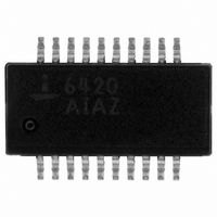
IC CTRLR PWM SYNC BUCK 20-QSOP
Manufacturer
Intersil
Specifications of ISL6420AIAZ-TK
Pwm Type
Voltage Mode
Number Of Outputs
1
Frequency - Max
1.4MHz
Duty Cycle
100%
Voltage - Supply
4.5 V ~ 28 V
Buck
Yes
Boost
No
Flyback
No
Inverting
No
Doubler
No
Divider
No
Cuk
No
Isolated
No
Operating Temperature
-40°C ~ 85°C
Package / Case
20-QSOP
Frequency-max
1.4MHz
Lead Free Status / RoHS Status
Lead free / RoHS Compliant
Other names
ISL6420AIAZ-TKTR
Available stocks
Company
Part Number
Manufacturer
Quantity
Price
Company:

Part Number:
ISL6420AIAZ-TK
Manufacturer:
Intersil
Quantity:
2 400


Pin Descriptions
VIN - This pin powers the controller and must be decoupled
to ground using a ceramic capacitor as close as possible to
the VIN pin.
SGND - This pin provides the signal ground for the IC. Tie
this pin to the ground plane through the lowest impedance
connection.
LGATE - This pin provides the PWM-controlled gate drive for
the lower MOSFET.
PHASE - This pin is the junction point of the output filter
inductor, the upper MOSFET source and the lower MOSFET
drain. This pin is used to monitor the voltage drop across the
upper MOSFET for overcurrent protection. This pin also
provides a return path for the upper gate drive.
UGATE - This pin provides the PWM-controlled gate drive
for the upper MOSFET.
BOOT - This pin powers the upper MOSFET driver. Connect
this pin to the junction of the bootstrap capacitor and the
cathode of the bootstrap diode. The anode of the bootstrap
diode is connected to the VCC5 pin.
FB - This pin is connected to the feedback resistor divider
and provides the voltage feedback signal for the controller.
This pin sets the output voltage of the converter.
COMP - This pin is the error amplifier output pin. It is used as
the compensation point for the PWM error amplifier.
PGOOD - This pin provides a power good status. It is an
open collector output used to indicate the status of the
output voltage.
RT - This is the oscillator frequency selection pin.
Connecting this pin directly to VCC5 will select the oscillator
free running frequency of 300kHz. By placing a resistor from
this pin to GND, the oscillator frequency can be programmed
from 100kHz to 1.4MHz. Figure 8 shows the oscillator
frequency vs the RT resistance.
CDEL - The PGOOD signal can be delayed by a time
proportional to a CDEL current of 2µA & the value of the
capacitor connected between this pin and ground. A 0.1µF
will typically provide 125ms delay. When in the Voltage
margining mode the CDEL current is 100µA typical and
provides the delay for the output voltage slew rate, 2.5ms
typical for the 0.1µF capacitor.
5.6V to 28V
5V ±10%
INPUT
TABLE 1. INPUT SUPPLY CONFIGURATION
Connect the input to the VIN pin. The VCC5
pin will provide a 5V output from the internal
LDO. Connect PVCC to VCC5.
Connect the input to the VCC5 pin. Connect
the PVCC and VIN pins to VCC5.
10
PIN CONFIGURATION
ISL6420A
PGND - This pin provides the power ground for the IC. Tie
this pin to the ground plane through the lowest impedance
connection.
PVCC - This pin is the power connection for the gate drivers.
Connect this pin to the VCC5 pin.
VCC5 – This pin is the output of the internal 5V LDO.
Connect a minimum of 4.7µF ceramic decoupling capacitor
as close to the IC as possible at this pin. Refer to Table 1.
ENSS - This pin provides enable/disable function and soft-
start for the PWM output. The output drivers are turned off
when this pin is held below 1V.
OCSET - Connect a resistor (ROCSET) from this pin to the
drain of the upper MOSFET. ROCSET, an internal 100µA
current source (IOCS), and the upper MOSFET on
resistance r
point according to the following equation:
An overcurrent trip cycles the soft-start function with an ON
time of 20ms and an OFF time of 128ms.
GPIO1/REFIN - This is a dual function pin. If VMSET/MODE
is not connected to VCC5 then this pin serves as GPIO1.
Refer to Table 2 for GPIO commands interpretation.
If VMSET/MODE is connected to VCC5 then this pin will
serve as REFIN. As REFIN, this pin is the non-inverting input
to the error amplifier. Connect the desired reference voltage
to this pin in the range of 0.6V to 1.25V.
Connect this pin to VCC5 to use internal reference.
REFOUT - If VMSET/MODE pin is connected to VCC5, then
this pin serves as REFOUT. It provides buffered reference
output for REFIN. Connect 2.2µF capacitor to this pin when
used as REFOUT. If not used to source current, connect a
1µF bypass capacitor to this pin.
I
OC
1400
1300
1200
1100
1000
=
900
800
700
600
500
400
300
200
100
I
------------------------------------------------------ -
0
OCSSET
FIGURE 8. OSCILLATOR FREQUENCY vs RT
0
DS(ON)
R
DS ON
•
(
25
R
OCSET
set the converter overcurrent (OC) trip
)
50
RT (kΩ)
75
100
125
October 13, 2005
FN9169.1
(EQ. 1)
150
Related parts for ISL6420AIAZ-TK
Image
Part Number
Description
Manufacturer
Datasheet
Request
R

Part Number:
Description:
Advanced Single Synchronous Buck Pulse-Width Modulation (PWM) Controller
Manufacturer:
Intersil
Datasheet:

Part Number:
Description:
Intersil Corporation [CMOS Serial Controller Interface]
Manufacturer:
Intersil Corporation
Datasheet:
Part Number:
Description:
Manufacturer:
Intersil Corporation
Datasheet:
Part Number:
Description:
357-036-542-201 CARDEDGE 36POS DL .156 BLK LOPRO
Manufacturer:
Intersil Corporation
Datasheet:
Part Number:
Description:
1024-Word x 4-Bit LSI Static RAM
Manufacturer:
Intersil Corporation
Datasheet:
Part Number:
Description:
General Purpose NPN Transistor Arrays FN341.4
Manufacturer:
Intersil Corporation
Datasheet:
Part Number:
Description:
CMOS 16-Bit Microprocessor
Manufacturer:
Intersil Corporation
Datasheet:
Part Number:
Description:
Manufacturer:
Intersil Corporation
Datasheet:
Part Number:
Description:
Manufacturer:
Intersil Corporation
Datasheet:
Part Number:
Description:
Manufacturer:
Intersil Corporation
Datasheet:
Part Number:
Description:
Manufacturer:
Intersil Corporation
Datasheet:
Part Number:
Description:
CMOS 6-Bit Latch and Decoder Memory Interfaces
Manufacturer:
Intersil Corporation
Datasheet:
Part Number:
Description:
CA3046General Purpose NPN Transistor Arrays
Manufacturer:
Intersil Corporation
Datasheet:
Part Number:
Description:
Manufacturer:
Intersil Corporation
Datasheet:
Part Number:
Description:
TR909 DLC/FLC SLIC with Low Power Standby
Manufacturer:
Intersil Corporation
Datasheet: