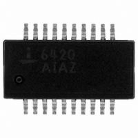
ISL6420AIAZ-TK Intersil, ISL6420AIAZ-TK Datasheet - Page 13

ISL6420AIAZ-TK
Manufacturer Part Number
ISL6420AIAZ-TK
Description
IC CTRLR PWM SYNC BUCK 20-QSOP
Manufacturer
Intersil
Specifications of ISL6420AIAZ-TK
Pwm Type
Voltage Mode
Number Of Outputs
1
Frequency - Max
1.4MHz
Duty Cycle
100%
Voltage - Supply
4.5 V ~ 28 V
Buck
Yes
Boost
No
Flyback
No
Inverting
No
Doubler
No
Divider
No
Cuk
No
Isolated
No
Operating Temperature
-40°C ~ 85°C
Package / Case
20-QSOP
Frequency-max
1.4MHz
Lead Free Status / RoHS Status
Lead free / RoHS Compliant
Other names
ISL6420AIAZ-TKTR
Available stocks
Company
Part Number
Manufacturer
Quantity
Price
Company:
Part Number:
ISL6420AIAZ-TK
Manufacturer:
Intersil
Quantity:
2 400
The slew time of the current is set by an external capacitor
on the CDEL pin, which is charged and discharged with a
100µA current source. The change in voltage on the
capacitor is 2.5V. This same capacitor is used to set the
PGOOD active delay after soft-start. When PGOOD is low,
the internal PGOOD circuitry uses the capacitor and when
PGOOD is high, the voltage margining circuit uses the
capacitor. The slew time for voltage margining can be in the
range of 300µs to 2ms.
External Reference/DDR Supply
The voltage margining can be disabled by connecting the
VMSET/MODE to VCC5. In this mode the chip can be
configured to work with an external reference input and
provide a buffered reference output.
If VMSET/MODE pin and the GPIO1/REFIN pin are both tied
to VCC5, then the internal 0.6V reference is used as the
error amplifier non-inverting input. The buffered reference
output on REFOUT will be 0.6V ±0.01V, capable of sourcing
V
V
IN
IN
= 12V, V
= 12V, V
OUT
OUT
FIGURE 11A.
FIGURE 11B.
= 3.3V, NO LOAD
= 3.3V, NO LOAD
13
ISL6420A
20mA and sinking up to 50µA current with a 2.2µF capacitor
connected to the REFOUT pin.
If VMSET/MODE pin is tied to high but GPIO1/REFIN is
connected to an external voltage source between 0.6V to
1.25V, then this external voltage is used as the reference
voltage at the positive input of the error amplifier. The
buffered reference output on REFOUT will be Vrefin ±0.01V,
capable of sourcing 20mA and sinking up to 50µA current
with a 2.2µF capacitor on the REFOUT pin.
Power Good
The PGOOD pin can be used to monitor the status of the
output voltage. PGOOD will be true (open drain) when the
FB pin is within ±10% of the reference and the ENSS pin has
completed its soft-start ramp.
Additionally, a capacitor on the CDEL pin will set a delay for
the PGOOD signal. After the ENSS pin completes its soft-
start ramp, a 2µA current begins charging the CDEL
capacitor to 2.5V. The capacitor will be quickly discharged
before PGOOD goes high. The programmable delay can be
used to sequence multiple converters or as a LOW-true
reset signal.
If the voltage on the FB pin exceeds ±10% of the reference,
then PGOOD will go low after 1µs of noise filtering.
Over-Temperature Protection
The IC is protected against over-temperature conditions.
When the junction temperature exceeds 150°C, the PWM
shuts off. Normal operation is resumed when the junction
temperature is cooled down to 130°C.
Shutdown
When ENSS pin is below 1V, the regulator is disabled with
the PWM output drivers three-stated. When disabled, the IC
power will be reduced.
V
IN
= 12V, V
FIGURE 12. PGOOD DELAY
OUT
= 3.3V, I
OUT
= 10A
October 13, 2005
FN9169.1


