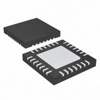
MAX5060ETI+T Maxim Integrated Products, MAX5060ETI+T Datasheet - Page 2

MAX5060ETI+T
Manufacturer Part Number
MAX5060ETI+T
Description
IC CNTRLR DC-DC 28-TQFN
Manufacturer
Maxim Integrated Products
Datasheet
1.MAX5061AUE.pdf
(31 pages)
Specifications of MAX5060ETI+T
Pwm Type
Current Mode
Number Of Outputs
1
Frequency - Max
1.5MHz
Duty Cycle
90%
Voltage - Supply
4.75 V ~ 28 V
Buck
Yes
Boost
No
Flyback
No
Inverting
No
Doubler
No
Divider
No
Cuk
No
Isolated
No
Operating Temperature
-40°C ~ 85°C
Package / Case
28-TQFN Exposed Pad
Frequency-max
1.5MHz
Output Voltage
0.6 V to 5.5 V
Output Current
30 A
Input Voltage
4.75 V to 5.5 V, 7 V to 28 V
Mounting Style
SMD/SMT
Maximum Operating Temperature
+ 85 C
Minimum Operating Temperature
- 40 C
Lead Free Status / RoHS Status
Lead free / RoHS Compliant
ABSOLUTE MAXIMUM RATINGS
IN to SGND.............................................................-0.3V to +30V
BST to SGND..........................................................-0.3V to +35V
DH to LX .......................................-0.3V to [(V
DL to PGND (MAX5060).............................-0.3V to (V
DL to PGND (MAX5061).............................-0.3V to (V
BST to LX..................................................................-0.3V to +6V
V
V
SGND to PGND .....................................................-0.3V to +0.3V
Current Sink in PGOOD ........................................................6mA
0.6V to 5.5V Output, Parallelable,
Average-Current-Mode DC-DC Controllers
ELECTRICAL CHARACTERISTICS
(V
(Note 1)
*Per JEDEC 51 standard.
Stresses beyond those listed under “Absolute Maximum Ratings” may cause permanent damage to the device. These are stress ratings only, and functional
operation of the device at these or any other conditions beyond those indicated in the operational sections of the specifications is not implied. Exposure to
absolute maximum rating conditions for extended periods may affect device reliability.
2
SYSTEM SPECIFICATIONS
Input Voltage Range
Quiescent Supply Current
Efficiency
OUTPUT VOLTAGE
SENSE+ to SENSE- Accuracy
(MAX5060) (Note 2)
Soft-Start Time
EAN Reference Voltage
(MAX5061)
STARTUP/INTERNAL REGULATOR
V
V
Hysteresis
V
MOSFET DRIVERS
Output-Driver Impedance
Output-Driver Source/Sink Current
Nonoverlap Time
CC
CC
CC
CC
CC
CC
, V
_______________________________________________________________________________________
to SGND............................................................-0.3V to +6V
= 5V, V
Undervoltage Lockout
Undervoltage Lockout
Output Voltage
DD
to PGND ...................................................-0.3V to +6V
PARAMETER
DD
= V
CC
(MAX5060 only), T
SYMBOL
I
DH_
UVLO
V
A
R
t
V
t
REF
NO
I
SS
ON
, I
= T
IN
Q
BST
DL_
J
- V
= T
LX_
DD
CC
MIN
Short IN and V
operation
EN = V
I
No load, V
f
No load, V
No load, V
no switching
No load, V
V
V
Low or high output,
I
C
) + 0.3V]
LOAD
SW
SOURCE/SINK
CC
IN
DH/DL
+ 0.3V)
+ 0.3V)
to T
= 7V to 28V, I
= 500kHz
rising
= 20A, V
MAX
CC
= 5nF
or SGND, not switching
CC
IN
CC
IN
, unless otherwise noted. Typical specifications are at T
CONDITIONS
= 7V to 28V, f
= 7V to 28V, no switching
= 4.75V to 5.5V,
= 4.75V to 5.5V,
= 20mA
CC
IN
All Other Pins to SGND...............................-0.3V to (V
Continuous Power Dissipation (T
Operating Temperature Range
Maximum Junction Temperature .....................................+150°C
Storage Temperature Range .............................-60°C to +150°C
Lead Temperature (soldering, 10s) .................................+300°C
SOURCE
16-Pin TSSOP (derate 21.3mW/°C above +70°C)* ......1702mW
28-Pin TQFN (derate 34.5mW/°C above +70°C)* ......2758mW
MAX5060A_ _ and MAX5061A_ _ .................-40°C to +125°C
MAX5060E_ _ and MAX5061E_ _ ....................-40°C to +85°C
= 12V, V
together for 5V input
= 0 to 60mA
OUT
SW
= 500kHz
= 3.3V
0.594
0.594
0.591
0.591
MIN
4.75
4.85
4.1
7
A
= +70°C)
1024
TYP
200
2.7
0.6
0.6
0.6
0.6
4.3
5.1
1.1
90
35
4
0.606
0.606
0.606
0.606
MAX
5.50
5.30
5.5
4.5
28
3
A
CC
= +25°C.)
Cycles
UNITS
Clock
+ 0.3V)
mA
mV
ns
%
V
V
V
V
V
A


