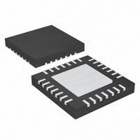
MAX5060ETI+T Maxim Integrated Products, MAX5060ETI+T Datasheet - Page 24

MAX5060ETI+T
Manufacturer Part Number
MAX5060ETI+T
Description
IC CNTRLR DC-DC 28-TQFN
Manufacturer
Maxim Integrated Products
Datasheet
1.MAX5061AUE.pdf
(31 pages)
Specifications of MAX5060ETI+T
Pwm Type
Current Mode
Number Of Outputs
1
Frequency - Max
1.5MHz
Duty Cycle
90%
Voltage - Supply
4.75 V ~ 28 V
Buck
Yes
Boost
No
Flyback
No
Inverting
No
Doubler
No
Divider
No
Cuk
No
Isolated
No
Operating Temperature
-40°C ~ 85°C
Package / Case
28-TQFN Exposed Pad
Frequency-max
1.5MHz
Output Voltage
0.6 V to 5.5 V
Output Current
30 A
Input Voltage
4.75 V to 5.5 V, 7 V to 28 V
Mounting Style
SMD/SMT
Maximum Operating Temperature
+ 85 C
Minimum Operating Temperature
- 40 C
Lead Free Status / RoHS Status
Lead free / RoHS Compliant
0.6V to 5.5V Output, Parallelable,
Average-Current-Mode DC-DC Controllers
The switching frequency, peak inductor current, and
allowable ripple at the output determine the value and
size of the inductor. Selecting higher switching frequen-
cies reduces the inductance requirement, but at the
cost of lower efficiency. The charge/discharge cycle of
the gate and drain capacitances in the switching
MOSFETs create switching losses. The situation wors-
ens at higher input voltages, since switching losses are
proportional to the square of the input voltage. The
MAX5060 can operate up to 1.5MHz, however for V
+12V, use lower switching frequencies to limit the
switching losses.
Use the following equation to determine the minimum
inductance value:
Choose I
current. Since I
inductance value may need minor adjustment after
choosing the output capacitors. Higher values reduce
the output ripple, but at the cost of degraded transient
response. Lower values have higher output ripple but
better transient response. Also, lower inductor values
correspond to smaller magnetics.
Choose inductors from the standard high-current, surface-
mount inductor series available from various manufac-
turers. Particular applications may require custom-
made inductors. Use high-frequency core material for
custom inductors. High I
flux excursion, which increases the core losses at higher
frequencies. The high-frequency operation coupled with
high I
even makes the use of planar inductors possible. The
advantages of using planar magnetics include low-profile
design, excellent current-sharing between modules due
to the tight control of parasitics, and low cost.
For example, calculate the minimum inductance at
V
330kHz:
24
IN(MAX)
______________________________________________________________________________________
L
reduces the required minimum inductance and
= 13.2V, V
L
L
L
MIN
MIN
equal to approximately 40% of the output
Applications Information
L
13 2
affects the output-ripple voltage, the
V
13 2 1 8
V
OUT
.
INMAX
INMAX
.
= 1.8V, I
L
330
.
causes large peak-to-peak
V
k
OUT
Inductor Selection
f
1 8
SW
.
8
L
V
= 8A, and f
0 6
OUT
.
I
L
H
SW
IN
>
=
The average-current-mode control feature of the
MAX5060/MAX5061 limits the maximum peak inductor
current and prevents the inductor from saturating. Choose
an inductor with a saturating current greater than the
worst-case peak inductor current. The hiccup current-limit
circuit is masked during startup to avoid unintentional
hiccup when large output capacitors are used.
Use the following equation to determine the worst-case
inductor current:
where R
When choosing a MOSFET for voltage regulators, con-
sider the total gate charge, R
and package thermal impedance. The product of the
MOSFET gate charge and on-resistance is a figure of
merit, with a lower number signifying better perfor-
mance. Choose MOSFETs optimized for high-frequen-
cy switching applications.
The average current from the MAX5060/MAX5061 gate-
drive output is proportional to the total capacitance it
drives at DH and DL. The power dissipated in the
MAX5060/MAX5061 is proportional to the input voltage
and the average drive current. See the IN, V
V
charge allowed from the combined driver outputs.
The gate charge and drain capacitance (CV 2) loss, the
cross-conduction loss in the upper MOSFET due to finite
rise/fall time, and the I 2 R loss due to RMS current in the
MOSFET R
MOSFET. Estimate the power loss (PD
the high-side and low-side MOSFETs using the following
equations:
where Q
MOSFET’s total gate charge, on-resistance at +25°C,
rise time, and fall time, respectively.
DD
V
IN
section to determine the maximum total gate
I
S
OUT
G
is the sense resistor and V
, R
PD
DS(ON)
DS(ON)
MOS HI
4
t
R
L
LPEAK
account for the total losses in the
t
, t
F
R
, and t
Q
f
SW
G
V
R
DS(ON)
CL
Switching MOSFETs
F
S
V
are the upper-switching
1 4
DD
.
R
2
DS ON
, power dissipation,
I
CL
L
MOS_
(
f
= 0.0282V.
SW
)
) caused by
I
2
RMS HI
CC
, and


