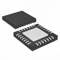
MAX5060ETI+T Maxim Integrated Products, MAX5060ETI+T Datasheet - Page 27

MAX5060ETI+T
Manufacturer Part Number
MAX5060ETI+T
Description
IC CNTRLR DC-DC 28-TQFN
Manufacturer
Maxim Integrated Products
Datasheet
1.MAX5061AUE.pdf
(31 pages)
Specifications of MAX5060ETI+T
Pwm Type
Current Mode
Number Of Outputs
1
Frequency - Max
1.5MHz
Duty Cycle
90%
Voltage - Supply
4.75 V ~ 28 V
Buck
Yes
Boost
No
Flyback
No
Inverting
No
Doubler
No
Divider
No
Cuk
No
Isolated
No
Operating Temperature
-40°C ~ 85°C
Package / Case
28-TQFN Exposed Pad
Frequency-max
1.5MHz
Output Voltage
0.6 V to 5.5 V
Output Current
30 A
Input Voltage
4.75 V to 5.5 V, 7 V to 28 V
Mounting Style
SMD/SMT
Maximum Operating Temperature
+ 85 C
Minimum Operating Temperature
- 40 C
Lead Free Status / RoHS Status
Lead free / RoHS Compliant
Use the following equation to calculate the resistor R
C
a midband zero. Place a zero (f
bump at the crossover frequency. Place a high-fre-
quency pole (f
crossover frequency to reduce the influence of the
switching noise and achieve maximum phase margin.
Use the following equations to calculate C
The TQFN-28 and TSSOP-16 are thermally enhanced
packages and can dissipate about 2.7W and 1.7W,
respectively. The high-power packages make the high-
frequency, high-current buck converter possible to
operate from a 12V or 24V bus. Calculate power dissi-
pation in the MAX5060/MAX5061 as a product of the
input voltage and the total V
(I
drive current (I
where Q
low-side and high-side external MOSFETs at V
5V, I
vs. Frequency graph in the Typical Operating
Characteristics, and f
the converter.
Use the following equation to calculate the maximum
power dissipation (P
ent temperature (T
MAX5060:
MAX5061:
CC
CF
). I
provides a low-frequency pole while R
Q
CC
is estimated from the Supply Current (I
P
P
G1
DMAX
DMAX
includes quiescent current (I
I
and Q
CC
C
C
DD
CF
CFF
R
= 34.5 x (150 - T
= 21.3 x (150 - T
P
= I
Average-Current-Mode DC-DC Controllers
CF
):
) at least a decade away from the
A
______________________________________________________________________________________
Q
G2
) :
P
DMAX
+ [f
2
D
SW
2
are the total gate charge of the
f
SW
= V
SW
V
is the switching frequency of
) in the chip at a given ambi-
OUT
IN
x (Q
CC
x I
1
L
f
Z
1
regulator output current
f
Power Dissipation
CC
G1
P
A
A
Z
R
)..............mW
)..............mW
0.6V to 5.5V Output, Parallelable,
) to obtain a phase
10
+ Q
S
R
R
CF
2
CF
G2
CF
)]
Q
) and gate-
CF
and C
provides
GATE
CFF
CF
Q
=
:
:
)
Use the following guidelines to layout the switching
voltage regulator.
1) Place the IN, V
2) Minimize the area and length of the high-current
3) Keep short the current loop formed by the lower
4) Place the Schottky diodes close to the lower
5) Keep the SGND and PGND isolated and connect
6) Run the current-sense lines CSP and CSN very
7) Avoid long traces between the V
8) Place the bank of output capacitors close to the load.
9) Distribute the power components evenly across the
10) Provide enough copper area at and around the
11) Use 4oz copper to keep the trace inductance and
close to the MAX5060/MAX5061.
loops from the input capacitor, upper switching
MOSFET, inductor, and output capacitor back to
the input capacitor negative terminal.
switching MOSFET, inductor, and output capacitor.
MOSFETs and on the same side of the PC board.
them at one single point close to the negative termi-
nal of the input filter capacitor.
close to each other to minimize the loop area.
Similarly, run the remote voltage sense lines
SENSE+ and SENSE- close to each other. Do not
cross these critical signal lines through power cir-
cuitry. Sense the current right at the pads of the
current-sense resistors.
(MAX5061) bypass capacitors, driver output of the
MAX5060/MAX5061, MOSFET gates, and PGND.
Minimize the loop formed by the V
capacitors, bootstrap diode, bootstrap capacitor,
MAX5060/MAX5061, and upper MOSFET gate.
board for proper heat dissipation.
switching MOSFETs, inductor, and sense resistors
to aid in thermal dissipation.
resistance to a minimum. Thin copper PC boards
can compromise efficiency since high currents are
involved in the application. Also, thicker copper
conducts heat more effectively, thereby reducing
thermal impedance.
CC
, and V
DD
PC Board Layout
bypass capacitors
DD
(MAX5060)/V
CC
bypass
CC
27


