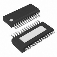
MAX8538EEI+ Maxim Integrated Products, MAX8538EEI+ Datasheet - Page 16

MAX8538EEI+
Manufacturer Part Number
MAX8538EEI+
Description
IC CNTRLR BUCK DUAL 28-QSOP
Manufacturer
Maxim Integrated Products
Datasheet
1.MAX8538EEI.pdf
(23 pages)
Specifications of MAX8538EEI+
Applications
Controller, DDR
Voltage - Input
4.5 ~ 23 V
Number Of Outputs
2
Voltage - Output
0.8 ~ 3.6 V
Operating Temperature
0°C ~ 85°C
Mounting Type
Surface Mount
Package / Case
28-QSOP
Output Voltage
0.8 V to 3.6 V
Output Current
30 A
Input Voltage
4.5 V to 23 V
Mounting Style
SMD/SMT
Maximum Operating Temperature
+ 85 C
Minimum Operating Temperature
- 40 C
Case
SSOP
Dc
05+
Lead Free Status / RoHS Status
Lead free / RoHS Compliant
Dual-Synchronous Buck Controllers for Point-of-
Load, Tracking, and DDR Memory Power Supplies
venting the output capacitor voltage from further devia-
tion from its regulating value.
Do not exceed the capacitor’s voltage or ripple
current ratings.
The MAX8537/MAX8538/MAX8539 controllers drive two
external, logic-level, N-channel MOSFETs as the circuit-
switch elements. The key selection parameters are:
1) On-resistance (R
2) Maximum drain-to-source voltage (V
3) Gate charges (Q
Choose MOSFETs with R
a good compromise between efficiency and cost,
choose the high-side MOSFET that has conduction loss
equal to the switching loss at the nominal input voltage
and maximum output current. For the low-side MOSFET,
make sure it does not spuriously turn on due to dV/dt
caused by the high-side MOSFET turning on, as this
results in shoot-through current degrading the efficiency.
MOSFETs with a lower Q
nity to dV/dt.
For proper thermal-management design, the power dis-
sipation must be calculated at the desired maximum
operating junction temperature, maximum output cur-
rent, and worst-case input voltage (for low-side
MOSFET, worst case is at V
MOSFET, it could be either at V
High-side and low-side MOSFETs have different loss
components due to the circuit operation. The low-side
MOSFET, operates as a zero-voltage switch; therefore,
the major losses are the channel conduction loss
(P
Use R
where V
the dead-time between the high-side MOSFET and the
low-side MOSFET switching transitions, and f
switching frequency.
The high-side MOSFET operates as a duty-cycle control
switch and has the following major losses: the channel
conduction loss (P
loss (P
MOSFET does not have body-diode conduction loss
because the diode never conducts current.
16
LSCC
at least 20% higher than the input supply rail at the
high-side MOSFET’s drain.
P
______________________________________________________________________________________
LSCC
DS,ON
HSSW
) and the body-diode conduction loss (P
F
is the body-diode forward voltage drop, t
= [1 - (V
P
), and the drive loss (P
at T
LSDC
J(MAX)
= 2 x I
HSCC
g
OUT
DS(ON)
, Q
:
gd
), the V I overlapping switching
/ V
DS(ON)
gd
LOAD
, Q
): the lower, the better.
/Q
IN
)] x (I
gs
gs
x V
): the lower, the better.
MOSFET Selection
IN(MAX)
rated at V
ratio have higher immu-
LOAD
F
IN(MIN)
HSDR
x t
dt
)
DSS
; for high-side
). The high-side
2
x f
GS
x R
or V
S
): should be
= 4.5V. For
DS,ON
IN(MAX)
LSDC
S
is the
dt
):
is
).
Use R
where I
current capability determined by:
where R
on-resistance (1.1Ω typ) and R
resistance of the MOSFET (~2Ω):
where V
In addition to the losses above, approximately 20% more
for additional losses due to MOSFET output capaci-
tances and low-side MOSFET body-diode reverse-recov-
ery charge dissipated in the high-side MOSFET that
exists, but is not well defined in the MOSFET data sheet.
Refer to the MOSFET data sheet for thermal-resistance
specification to calculate the PC board area needed to
maintain the desired maximum operating junction tem-
perature with the above-calculated power dissipation.
To reduce EMI caused by switching noise, add a 0.1µF
ceramic capacitor from the high-side switch drain to
the low-side switch source or add resistors in series
with DH and DL to slow down the switching transitions.
However, adding series resistors increases the power
dissipation of the MOSFETs, so be sure this does not
overheat the MOSFETs.
The minimum load current must exceed the high-side
MOSFET’s maximum leakage current over temperature
if fault conditions are expected.
The MAX8537/MAX8538/MAX8539 controllers sense
the peak inductor current to provide constant current
and hiccup current limit. The peak current-limit thresh-
old is set by an external resistor together with the inter-
nal current sink of 200µA. The voltage drop across the
resistor R
maximum peak inductor current that can flow through
the high-side MOSFET or the optional current-sense
resistor by the equations below:
or
R
limit accuracy. The actual corresponding maximum
load current is lower than the I
ILIM_
P
P
HSDR
HSSW
I
PEAK(MAX)
DS(ON)
P
should be less than 1.5kΩ for optimum current-
GATE
GS
HSCC
DH
I
PEAK(MAX)
ILIM_
= Q
= V
~ VL = 5V
I
GATE(ON)
is the high-side MOSFET driver’s average
at T
gs
IN
is the average DH-high driver output-
= (V
with 200µA current through it sets the
x I
x V
= 200µA x R
J(MAX):
OUT
LOAD
GS
= 200µA x R
.
= 2.5 / (R
/ V
x f
x f
S
IN
S
x R
) x I
Current-Limit Setting
x [(Q
ILIM_
GATE
PEAK(MAX)
GATE
DH
2
LOAD
ILIM_
gs
/ R
+ R
/ (R
is the internal gate
+ Q
DSON(HSFET)
/ R
GATE
x R
GATE
gd
SENSE
DS(ON)
above by half
) / I
)
+ R
GATE
DH
]
)


