ISL6314IRZ Intersil, ISL6314IRZ Datasheet
ISL6314IRZ
Specifications of ISL6314IRZ
Available stocks


Related parts for ISL6314IRZ

ISL6314IRZ Summary of contents
Page 1
... PART NUMBER PART (Note) MARKING ISL6314CRZ* ISL6314 CRZ ISL6314IRZ* ISL6314 IRZ *Add “-T” suffix for tape and reel. Please refer to TB347 for details on reel specifications. NOTE: These Intersil Pb-free plastic packaged products employ special Pb-free material sets, molding compounds/die attach ...
Page 2
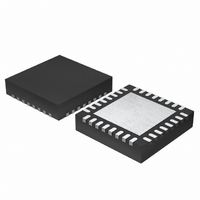
Pinout PGOOD COMP ISL6314 Integrated Driver Block Diagram PWM SOFT-START AND FAULT LOGIC 2 ISL6314 ISL6314 ISL6314 (32 LD QFN) TOP VIEW REF 4 33 GND OFS 5 ...
Page 3
Block Diagram ISENO ISEN- ISEN+ ISEN AMP RGND VSEN x1 FSD VDIFF OPEN SENSE LINE DETECT UNDERVOLTAGE DETECTION LOGIC OVERVOLTAGE DETECTION LOGIC FS/DROOP FS SELECT MODE/DAC SS SELECT VID7 VID6 VID5 DYNAMIC VID4 VID D/A VID3 VID2 VID1 2kΩ VID0 ...
Page 4
Typical Application - ISL6314 FB DVC COMP APA +5V VCC OFS FS REF SS VID7 VID6 VID5 VID4 VID3 VID2 VID1 VID0 PGOOD EN ISEN+ OCSET R OCSET 4 ISL6314 ISL6314 VDIFF VSEN RGND Typical Applications 1. PVCC = 12V; ...
Page 5
Typical Application - ISL6314 with NTC Thermal Compensation FB DVC COMP APA +5V VCC OFS FS REF SS VID7 VID6 VID5 VID4 VID3 VID2 VID1 VID0 PGOOD EN ISEN+ OCSET R OCSET 5 ISL6314 ISL6314 VDIFF VSEN RGND +12V PVCC ...
Page 6
... V + 0.3V http://www.intersil.com/pbfree/Pb-FreeReflow.asp BOOT + 0.3V BOOT Recommended Operating Conditions VCC Supply Voltage . . . . . . . . . . . . . . . . . . . . . . . . . . . . . .+5V ±5% PVCC Supply Voltage . . . . . . . . . . . . . . . . . . . . . . . +5V to 12V ±5% Ambient Temperature ISL6314CRZ . . . . . . . . . . . . . . . . . . . . . . . . . . . . . . 0°C to +70°C ISL6314IRZ . . . . . . . . . . . . . . . . . . . . . . . . . . . . . .-40°C to +85°C TEST CONDITIONS 5V high, VCC CC not switching PVCC = 12V high, PVCC high, not switching ...
Page 7
... Maximum Output Voltage Minimum Output Voltage SOFT-START RAMP Soft-Start Ramp Rate Adjustment Range of Soft-Start Ramp Rate (Note 3) OVERCURRENT PROTECTION OCSET Trip Current (ISL6314CRZ) OCSET Trip Current (ISL6314IRZ) OCSET Accuracy ISENO Offset PROTECTION Undervoltage Threshold Undervoltage Hysteresis Overvoltage Threshold During Soft-Start Overvoltage Threshold (Default) ...
Page 8
Electrical Specifications Recommended Operating Conditions, Unless Otherwise Specified. Parameters with MIN and/or MAX limits are 100% tested at +25°C, unless otherwise specified. Temperature limits established by characterization and are not production tested. (Continued) PARAMETER SWITCHING TIME (Note 3) UGATE Rise ...
Page 9
Functional Pin Description VCC (Pin 18) VCC is the bias supply for the ICs small-signal circuitry. Connect this pin to a +5V supply and decouple using a quality 0.1µF ceramic capacitor. PVCC (Pin 19) This pin is the power supply ...
Page 10
... Equation 2 shows the approximation for the output voltage ripple P-P Adaptive Phase Alignment (APA) To improve the transient response, the ISL6314 implements Intersil’s proprietary Adaptive Phase Alignment (APA) technique, which turns on the channel during large current step transient events. IL, 7A/DIV PWM, 5V/DIV 1µs/DIV FOR 1-PHASE CONVERTER ) V ⋅ ...
Page 11
... FS pin. The advantage of Intersil’s proprietary Active Pulse Positioning (APP) modulator is that the PWM signal has the ability to turn on at any point during this PWM time interval, and turn off immediately after the PWM signal has transitioned high ...
Page 12
TABLE 1. ISL6314 DAC SELECT AND FUNCTION TABLE DAC VERSION SS PIN INTEL VR11 R resistor tied to SS GND AMD 5-BIT R resistor tied to SS VCC AMD 6-BIT R resistor tied to SS VCC TIE RESISTOR to OPEN ...
Page 13
TABLE 2. VR11 VOLTAGE IDENTIFICATION CODES (Continued) VID7 VID6 VID5 VID4 VID3 VID2 VID1 VID0 ...
Page 14
TABLE 2. VR11 VOLTAGE IDENTIFICATION CODES (Continued) VID7 VID6 VID5 VID4 VID3 VID2 VID1 VID0 ...
Page 15
... DAC) and 0 0.8000 offset errors in the OFS current source, remote-sense and error amplifiers. Intersil specifies the guaranteed tolerance of 1 0.7750 the ISL6314 to include the combined tolerances of each of 0 0.7625 these elements. ...
Page 16
The output of the error amplifier, V COMP sawtooth waveform to generate the PWM signal. The PWM signal controls the timing of the Internal MOSFET drivers and regulates the converter output so that the voltage equal to ...
Page 17
R COMP ⋅ ⋅ -------------------- - DCR DROOP OUT simply adjusting the value the load line can be set S to any level, giving the converter the right amount of ...
Page 18
Dynamic VID Modern microprocessors need to make changes to their core voltage as part of normal operation. They direct the ISL6314 to do this by making changes to the VID inputs. The ISL6314 is required to monitor the DAC inputs ...
Page 19
DVC ------- - C = DVC A Advanced Adaptive Zero Shoot-Through Deadtime Control (Patent Pending) The integrated drivers incorporate a unique adaptive deadtime control technique to minimize deadtime, resulting in high efficiency ...
Page 20
ISL6314 INTERNAL CIRCUIT POR ENABLE CIRCUIT COMPARATOR + - 0.85V SOFT-START AND FAULT LOGIC FIGURE 10. POWER SEQUENCING USING THRESHOLD-SENSITIVE ENABLE (EN) FUNCTION Enable and Disable While in shutdown mode, the LGATE and UGATE signals are held low to ...
Page 21
– 3 ⋅ ⋅ ⋅ ( μ – 1 VID SS For example, when VID is ...
Page 22
R OCSET - ISENO V OCSET ISEN+ + ISEN - - V DROOP ISEN VDIFF - +1V VID + OFFSET mV SOFT-START, FAULT AND CONTROL LOGIC V OVP - OV VSEN + + ...
Page 23
... The first step in designing a power converter using the ISL6314 is to determine if one phase is sufficient (if not, Intersil offers other parts, such as the ISL6313, which has two phases with similar features). This determination depends heavily on the cost analysis which in turn depends on system constraints that differ from one design to the next. ...
Page 24
LOWER MOSFET POWER CALCULATION The calculation for power loss in the lower MOSFET is simple, since virtually all of the loss in the lower MOSFET is due to current conducted through the channel resistance ( Equation 21, I ...
Page 25
VCC Qg_TOT Qg_Q1 Qg_Q2 Q 3 ⋅ ⋅ ⋅ PVCC F = Qg_Q1 ⋅ ⋅ ⋅ PVCC Qg_Q2 G2 ...
Page 26
Choose an arbitrary value for C COMP value is 0.01µF. 2. Plug the inductor L and DCR component values, and the values for C chosen in Step 1, into Equation 30 to COMP calculate the value for R . ...
Page 27
C (OPTIONAL COMP VDIFF FIGURE 20. COMPENSATION CONFIGURATION FOR LOAD-LINE REGULATED ISL6314 CIRCUIT Since the system poles and zero are affected by the values of the components that are meant to compensate ...
Page 28
COMP VDIFF FIGURE 21. COMPENSATION CIRCUIT WITHOUT LOAD-LINE REGULATION . ⋅ C ESR ⋅ ------------------------------------------- - ⋅ ⋅ – C ...
Page 29
Normally, the trailing edge dictates the selection of L because duty cycles are usually less than 50%. Nevertheless, both inequalities should be evaluated, and L should be selected based on the lower of the two results. ...
Page 30
... Accordingly, the reader is cautioned to verify that data sheets are current before placing orders. Information furnished by Intersil is believed to be accurate and reliable. However, no responsibility is assumed by Intersil or its subsidiaries for its use; nor for any infringements of patents or other rights of third parties which may result from its use ...
Page 31
R FB LOCATE CLOSE TO IC (MINIMIZE CONNECTION PATH DVC C DVC FB DVC VDIFF VSEN COMP C APA APA R APA +5V VCC (CF1) R OFS OFS FS ...
Page 32
Package Outline Drawing L32.5x5B 32 LEAD QUAD FLAT NO-LEAD PLASTIC PACKAGE Rev 2, 11/07 5.00 6 PIN 1 INDEX AREA (4X) 0.15 TOP VIEW ( 4. 80 TYP ) ( TYPICAL RECOMMENDED LAND PATTERN 32 ISL6314 A ...