ISL6314IRZ Intersil, ISL6314IRZ Datasheet - Page 24
ISL6314IRZ
Manufacturer Part Number
ISL6314IRZ
Description
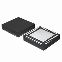
IC CTRLR PWM 1PHASE BUCK 32-QFN
Manufacturer
Intersil
Datasheet
1.ISL6314CRZ.pdf
(32 pages)
Specifications of ISL6314IRZ
Applications
Controller, Intel VR11, AMD CPU
Voltage - Input
5 ~ 12 V
Number Of Outputs
1
Voltage - Output
0.38 ~ 1.6 V
Operating Temperature
-40°C ~ 85°C
Mounting Type
Surface Mount
Package / Case
32-VQFN Exposed Pad, 32-HVQFN, 32-SQFN, 32-DHVQFN
Lead Free Status / RoHS Status
Lead free / RoHS Compliant
Available stocks
Company
Part Number
Manufacturer
Quantity
Price
Company:

Part Number:
ISL6314IRZ-T
Manufacturer:
ALTERA
Quantity:
5
Part Number:
ISL6314IRZ-T
Manufacturer:
INTERSIL
Quantity:
20 000


LOWER MOSFET POWER CALCULATION
The calculation for power loss in the lower MOSFET is
simple, since virtually all of the loss in the lower MOSFET is
due to current conducted through the channel resistance
(r
output current, I
Equation 1), and d is the duty cycle (V
An additional term can be added to the lower-MOSFET loss
equation to account for additional loss accrued during the dead
time when inductor current is flowing through the
lower-MOSFET body diode. This term is dependent on the
diode forward voltage at I
f
and the end of the lower-MOSFET conduction interval
respectively. Note that the dead times t
Equation 22 are NOT related to the soft-start timing delays.
The total maximum power dissipated in each lower MOSFET
is approximated by the summation of P
UPPER MOSFET POWER CALCULATION
In addition to r
upper-MOSFET losses are due to currents conducted across
the input voltage (V
higher portion of the upper-MOSFET losses are dependent on
switching frequency, the power calculation is more complex.
Upper MOSFET losses can be divided into separate
components involving the upper-MOSFET switching times,
the lower-MOSFET body-diode reverse-recovery charge, Q
and the upper MOSFET r
When the upper MOSFET turns off, the lower MOSFET does
not conduct any portion of the inductor current until the
voltage at the phase node falls below ground. Once the
lower MOSFET begins conducting, the current in the upper
MOSFET falls to zero as the current in the lower MOSFET
ramps up to assume the full inductor current. In Equation 23,
the required time for this commutation is t
approximated associated power loss is P
At turn on, the upper MOSFET begins to conduct and this
transition occurs over a time t
approximate power loss is P
S
P
P
P
P
DS(ON)
, and the length of dead times, t
LOW 2 ( )
LOW 1 ( )
UP 1 ( )
UP 2 ( )
≈
≈
). In Equation 21, I
=
V
V
=
IN
IN
V
r
D ON
DS ON
⋅
DS(ON)
⋅
(
⎛
⎝
⎛
⎜
⎝
I
----- -
PP
(
I
----- -
N
N
M
M
)
+
–
⋅
IN
is the peak-to-peak inductor current (see
)
f
I
--------- -
I
--------- -
⋅
S
P-P
P-P
) during switching. Since a substantially
2
2
losses, a large portion of the
⋅
⎛
⎜
⎝
I
----- -
⎞
⎠
⎞
⎟
⎠
N
⎛
⎜
⎝
M
M
I M
------
DS(ON)
N
⋅
⋅
⎞
⎟
⎠
, V
⎛
⎜
⎝
⎛
⎜
⎝
2
+
M
t
----
t
----
2
2
2
⋅
1
UP(2).
D(ON)
I
-----------
24
(
P-P
⎞
⎟
⎠
⎞
⎟
⎠
is the maximum continuous
2
1 d
2
. In Equation 24, the
⋅
⋅
–
f
d1
f
⎞
⎟
⎠
S
conduction loss.
S
⋅
, the switching frequency,
.
)
t
and t
d1
+
d1
I
--------------------------------------- -
L P-P
OUT
+
(
LOW(1)
d2
⎛
⎜
⎜
⎝
and t
I M
------
N
UP(1).
1
, at the beginning
/V
2
)
12
–
and the
⋅
I
-----------
IN
d2
(
P-P
1 d
2
).
and P
.
–
in
⎞
⎟
⎟
⎠
⋅
)
t
d2
(EQ. 21)
(EQ. 22)
LOW(2)
(EQ. 24)
(EQ. 23)
rr
,
ISL6314
.
A third component involves the lower MOSFET
reverse-recovery charge, Q
fully commutated to the upper MOSFET before the
lower-MOSFET body diode can recover all of Q
conducted through the upper MOSFET across VIN. The
power dissipated as a result is P
25.
Finally, the resistive part of the upper MOSFET is given in
Equation 26 as P
The total power dissipated by the upper MOSFET at full load
can now be approximated as the summation of the results
from Equations 23, 24, 25 and 26. Since the power
equations depend on MOSFET parameters, choosing the
correct MOSFETs can be an iterative process involving
repetitive solutions to the loss equations for different
MOSFETs and different switching frequencies.
Package Power Dissipation
When choosing MOSFETs it is important to consider the
amount of power being dissipated in the integrated drivers
located in the controller. Since there is one set of drivers in
the controller package, the total power dissipated by it must
be less than the maximum allowable power dissipation for
the QFN package.
Calculating the power dissipation in the drivers for a desired
application is critical to ensure safe operation. Exceeding the
maximum allowable power dissipation level will push the IC
beyond the maximum recommended operating junction
temperature of +125°C. The maximum allowable IC power
dissipation for the 5x5 QFN package is approximately 3W at
room temperature. See “Layout Considerations” on page 29
for thermal transfer improvement suggestions.
When designing the ISL6314 into an application, it is
recommended that the following calculation is used to
ensure safe operation at the desired frequency for the
selected MOSFETs. The total gate drive power losses,
P
integrated driver’s internal circuitry and their corresponding
average driver current can be estimated with Equations 27
and 28, respectively.
P
P
Qg_TOT
UP 3 ( )
UP 4 ( )
=
≈
, due to the gate charge of MOSFETs and the
r
V
DS ON
IN
(
⋅
Q
)
rr
UP(4).
⋅
⋅
d
f
⋅
S
⎛
⎜
⎝
.
I
----- -
N
M
⎞
⎟
⎠
2
rr
+
. Since the inductor current has
I
--------- -
P-P
12
UP(3)
2
, as shown in Equation
rr
, it is
October 8, 2009
(EQ. 25)
(EQ. 26)
FN6455.2
Related parts for ISL6314IRZ
Image
Part Number
Description
Manufacturer
Datasheet
Request
R

Part Number:
Description:
Intersil Corporation [CMOS Serial Controller Interface]
Manufacturer:
Intersil Corporation
Datasheet:
Part Number:
Description:
Manufacturer:
Intersil Corporation
Datasheet:
Part Number:
Description:
357-036-542-201 CARDEDGE 36POS DL .156 BLK LOPRO
Manufacturer:
Intersil Corporation
Datasheet:
Part Number:
Description:
1024-Word x 4-Bit LSI Static RAM
Manufacturer:
Intersil Corporation
Datasheet:
Part Number:
Description:
General Purpose NPN Transistor Arrays FN341.4
Manufacturer:
Intersil Corporation
Datasheet:
Part Number:
Description:
CMOS 16-Bit Microprocessor
Manufacturer:
Intersil Corporation
Datasheet:
Part Number:
Description:
Manufacturer:
Intersil Corporation
Datasheet:
Part Number:
Description:
Manufacturer:
Intersil Corporation
Datasheet:
Part Number:
Description:
Manufacturer:
Intersil Corporation
Datasheet:
Part Number:
Description:
Manufacturer:
Intersil Corporation
Datasheet:
Part Number:
Description:
CMOS 6-Bit Latch and Decoder Memory Interfaces
Manufacturer:
Intersil Corporation
Datasheet:
Part Number:
Description:
CA3046General Purpose NPN Transistor Arrays
Manufacturer:
Intersil Corporation
Datasheet:
Part Number:
Description:
Manufacturer:
Intersil Corporation
Datasheet:
Part Number:
Description:
TR909 DLC/FLC SLIC with Low Power Standby
Manufacturer:
Intersil Corporation
Datasheet:
Part Number:
Description:
Manufacturer:
Intersil Corporation
Datasheet: