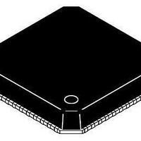
ADP3208DJCPZ-RL ON Semiconductor, ADP3208DJCPZ-RL Datasheet - Page 17

ADP3208DJCPZ-RL
Manufacturer Part Number
ADP3208DJCPZ-RL
Description
IC CTLR BUCK 7BIT 2PHASE 48LFCSP
Manufacturer
ON Semiconductor
Datasheet
1.ADP3208DJCPZ-RL.pdf
(37 pages)
Specifications of ADP3208DJCPZ-RL
Applications
Controller, Power Supplies for Next-Generation Intel Processors
Voltage - Input
3.3 ~ 22 V
Number Of Outputs
1
Voltage - Output
0.01 ~ 1.5 V
Operating Temperature
-10°C ~ 100°C
Mounting Type
Surface Mount
Package / Case
48-LFCSP
Output Voltage
10 mV
Output Current
40 A
Input Voltage
19 V
Supply Current
6 mA
Switching Frequency
300 KHz
Mounting Style
SMD/SMT
Maximum Operating Temperature
+ 100 C
Minimum Operating Temperature
- 10 C
Lead Free Status / RoHS Status
Lead free / RoHS Compliant
Available stocks
Company
Part Number
Manufacturer
Quantity
Price
Company:
Part Number:
ADP3208DJCPZ-RL
Manufacturer:
ON Semiconductor
Quantity:
10
Part Number:
ADP3208DJCPZ-RL
Manufacturer:
ON/安森美
Quantity:
20 000
Setting Switch Frequency
Master Clock Frequency in PWM Mode
connected from the RT pin to GND sets the clock frequency.
The frequency is constant at a given VID code but varies
with the VID voltage: the lower the VID voltage, the lower
the clock frequency. The variation of clock frequency with
VID voltage maintains constant V
power conversion efficiency at lower VID voltages.
Figure 15 shows the relationship between clock frequency
and VID voltage, parametrized by RT resistance.
the clock by the number of phases in use.
Switching Frequency in RPM Mode — Single−Phase
Operation
controlled by the ripple voltage on the COMP pin, rather
than by the master clock. Each time the COMP pin voltage
exceeds the RPM pin voltage threshold level determined by
the VID voltage and the external resistor connected from
RPM to GND, an internal ramp signal is started and DRVH1
is driven high. The slew rate of the internal ramp is
programmed by the current entering the RAMP pin.
One−third of the RAMP current charges an internal ramp
When the ADP3208D runs in PWM, an external resistor
To determine the switching frequency per phase, divide
In single−phase RPM mode, the switching frequency is
VCC
RAMP
I
I
R
R
= A
= A
R
R
C
C
y I
y I
R
R
RAMP
RAMP
A
A
D
D
OSCILLATOR
OSCILLATOR
COMP
CLOCK
CLOCK
0.2V
0.2V
CORE
R
A
C
FB
Figure 27. Dual−Phase PWM Mode Operation
C
ripple and improves
FB
A
+
R
+
C
B
V
B
VDC
+ –
CS
FBRTN
FLIP−FLOP
FLIP−FLOP
S
RD
RD
S
http://onsemi.com
Q
Q
LLINE
17
–
+
CSCOMP
capacitor (5 pF typical) and creates a ramp. When the
internal ramp signal intercepts the COMP voltage, the
DRVH1 pin is reset low.
RPM operation is almost constant. While in discontinuous
current conduction mode, the switching frequency is
reduced as a function of the load current.
Differential Sensing of Output Voltage
accuracy VID DAC, referenced by a precision band gap
source and a low offset error amplifier, to meet the rigorous
accuracy requirement of the Intel IMVP−6+ specification.
In steady−state mode, the combination of the VID DAC and
error amplifier maintain the output voltage for a worst−case
scenario within ±8 mV of the full operating output voltage
and temperature range.
and FBRTN pins. FB should be connected through a resistor
to the positive regulation point; the VCC remote sensing pin
of the microprocessor. FBRTN should be connected directly
to the negative remote sensing point; the V
of the CPU. The internal VID DAC and precision voltage
reference are referenced to FBRTN and have a maximum
current of 200 mA for guaranteed accurate remote sensing.
GATE DRIVER
GATE DRIVER
IN
In continuous current mode, the switching frequency of
The ADP3208D combines differential sensing with a high
The CPU core output voltage is sensed between the FB
DRVH
DRVH
DRVL
DRVL
BST
BST
SW
SW
CSSUM
5V
DRVH1
DRVH2
DRVL1
DRVL2
CSREF
R
C
BST2
BST1
SW1
SW2
CS
CS
5V
VCC
VCC
R
R
PH
PH
R
R I
I
L
L
SS
LOAD
sensing point
0 6 3 7 4 - 0 2 5


