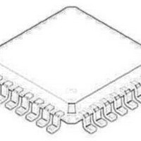
NCP5318FTR2G ON Semiconductor, NCP5318FTR2G Datasheet - Page 28

NCP5318FTR2G
Manufacturer Part Number
NCP5318FTR2G
Description
IC CTLR CPU 2/3/4 PHASE 32-LQFP
Manufacturer
ON Semiconductor
Datasheet
1.NCP5318FTR2G.pdf
(32 pages)
Specifications of NCP5318FTR2G
Applications
Controller, CPU
Voltage - Input
9.5 ~ 13.2 V
Number Of Outputs
4
Operating Temperature
0°C ~ 70°C
Mounting Type
Surface Mount
Package / Case
32-LQFP
Switching Frequency
1 MHz
Mounting Style
SMD/SMT
Primary Input Voltage
18V
No. Of Pins
32
Operating Temperature Range
0°C To +70°C
Termination Type
SMD
Supply Voltage Min
12V
Packaging Type
Tape And Reel
Peak Reflow Compatible (260 C)
Yes
Frequency
1MHz
Rohs Compliant
Yes
Lead Free Status / RoHS Status
Lead free / RoHS Compliant
Voltage - Output
-
Lead Free Status / Rohs Status
Lead free / RoHS Compliant
Other names
NCP5318FTR2G
NCP5318FTR2GOSTR
NCP5318FTR2GOSTR
Available stocks
Company
Part Number
Manufacturer
Quantity
Price
Company:
Part Number:
NCP5318FTR2G
Manufacturer:
ON Semiconductor
Quantity:
10 000
of the controller. At no load, this resistor will conduct the
very small internal bias current of the V
R
error due to the input bias current. If the R
small, the V
pins of the controller. At no load, V
at the same potential, and no current should flow through
R
V
voltage at V
pin close to the reference voltage. Figure 30 shows the
DC effect of AVP.
FB
DRP
DRP
−0.02
−0.04
−0.06
−0.08
−0.10
−0.12
−0.14
Resistor R
Resistor R
should be kept below 10 kW to avoid output voltage
0
or R
pin rises. The the R
Figure 30. The DC Effects of AVP vs. Load
0
Figure 31. Output Voltage − No Capacitor
FB
OUT
FB
FB
OUTPUT VOLTAGE, 50 mV/DIV
DRP
. As load current increases, the voltage at the
LOAD CURRENT, 60 A/DIV
10
bias current can be ignored.
VDRP VOLTAGE, 200 mV/DIV
is connected between V
to fall in order to keep the voltage at the V
is connected between the V
5 mS/DIV
in Parallel with R
20
Spec Min
Spec Max
DRP
I
OUT
and R
30
(A)
DRP
FB
DRP
OUT
40
, V
V
resistors cause the
OUT
FB
FB
FB
and the V
pin. Therefore
resistor is kept
− VID
and V
DRP
50
and V
OUT
http://onsemi.com
FB
60
pin
are
FB
FB
28
ratio based on the desired loadline and sense resistor. At no
load, the output voltage is positioned 19 mV below the DAC
output setting. The output voltage droop will follow the
equation:
where:
equation to find R
voltage droop divided by the output current. If a sense
resistor is used to detect inductor current, then R
be the value of the sense resistor. If inductor sensing is used,
R
discussion on Current Sensing for further information.
adding a capacitor on the order of 1 nF in parallel with R
may improve the transient output voltage waveshape.
SENSE
To choose components, select the appropriate resistor
It is easiest to select a value for R
Depending on inductor ESR and the loadline desired,
g = gain of the current sense amplifiers (V/V);
R
R
Figure 32. Output Voltage – 1.2 nF Capacitor
will be the resistance of the inductor. Refer to the
SENSE
LL
OUTPUT VOLTAGE, 50 mV/DIV
LOAD CURRENT, 60 A/DIV
= load line resistance (mW).
R DRP
VDRP VOLTAGE, 200 mV/DIV
R FB
5 mS/DIV
= resistance of the sense element (mW);
DRP
+ g
in Parallel with R
. R
LL
R SENSE
is simply the desired output
R LL
FB
and then evaluate the
DRP
SENSE
(eq. 30)
DRP
will


