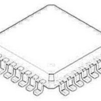
NCP5318FTR2G ON Semiconductor, NCP5318FTR2G Datasheet - Page 7

NCP5318FTR2G
Manufacturer Part Number
NCP5318FTR2G
Description
IC CTLR CPU 2/3/4 PHASE 32-LQFP
Manufacturer
ON Semiconductor
Datasheet
1.NCP5318FTR2G.pdf
(32 pages)
Specifications of NCP5318FTR2G
Applications
Controller, CPU
Voltage - Input
9.5 ~ 13.2 V
Number Of Outputs
4
Operating Temperature
0°C ~ 70°C
Mounting Type
Surface Mount
Package / Case
32-LQFP
Switching Frequency
1 MHz
Mounting Style
SMD/SMT
Primary Input Voltage
18V
No. Of Pins
32
Operating Temperature Range
0°C To +70°C
Termination Type
SMD
Supply Voltage Min
12V
Packaging Type
Tape And Reel
Peak Reflow Compatible (260 C)
Yes
Frequency
1MHz
Rohs Compliant
Yes
Lead Free Status / RoHS Status
Lead free / RoHS Compliant
Voltage - Output
-
Lead Free Status / Rohs Status
Lead free / RoHS Compliant
Other names
NCP5318FTR2G
NCP5318FTR2GOSTR
NCP5318FTR2GOSTR
Available stocks
Company
Part Number
Manufacturer
Quantity
Price
Company:
Part Number:
NCP5318FTR2G
Manufacturer:
ON Semiconductor
Quantity:
10 000
ELECTRICAL CHARACTERISTICS (continued)
C
VID Inputs
Power Good
Overvoltage Protection
Enable Input
Error Amplifier
PWM Comparators
MOSFET Driver Enable (DRVON)
2. Guaranteed by design, not tested in production.
SGND Bias Current
SGND Voltage Compliance Range
Upper Threshold Offset
Lower Threshold Ratio
Time to Assert PWRGD
Time to De−assert PWRGD
Output Low Voltage
OVP Threshold above VID
Start Threshold
Stop Threshold
Hysteresis
Input Pull−Up Voltage
Input Pull−Up Resistance
V
COMP Source Current
COMP Sink Current
Transconductance
Open Loop DC Gain
Unity Gain Bandwidth
PSRR @ 1.0 kHz
COMP Max Voltage
COMP Min Voltage
Minimum Pulse Width
Transient Response Time
Channel Startup Offset
Artificial Ramp Amplitude
Output High
Output Low
Pull−Down Resistance
SS
FB
= 0.1 mF, C
Bias Current
VCC
Characteristic
= 0.1 mF, R
ROSC
= 95.3 kW, V(I
SGND < 300 mV, All DAC Codes
Offset from the No Load Set Point Voltage
PWRLS Voltage / No Load Set Point Volt-
age
Delay from V
Delay from V
Low
Voltage with Open Collector Pin Sinking
4 mA
Gates switching, SS high
Gates not switching, SS low
1.0 MW to GND
COMP = 0.5 V to 2.0 V
C
V
V
Measured from CSxP to GATEx,
V
60 mV step between CSxP and CSxN;
Measure at GATEx = 1.0 V (Note 2)
Measured from CSxN to GATEx,
COMP = 2.1 V, CSxP = CSxN = 0.5 V,
CSxN stepped from 1.2 V to 2.0 V (Note 2)
CSxP = CSxN = V
when GATEx switch high
50% duty cycle
DRVON floating
I = 100 mA
DRVON = 1.5 V, ENABLE = 0 V,
R = 1.5 V/I(DRVON)
LIM
FB
FB
FB
COMP
) = 1.0 V, DAC Code 010100; unless otherwise noted)
= 0 V
= 1.6 V
= CSxN = 0.5, COMP = 0.5 V,
(0°C < T
http://onsemi.com
= 30 pF (Note 2)
OUT
OUT
Test Conditions
A
< 70°C; V
in Range to PWRGD High
out of Range to PWRGD
(Note 2)
(Note 2)
(Note 2)
7
FB
−
−
−
−
−
−
= 0, Measure Vcomp
CC
= 12 V; C
GATEx
= 100 pF, C
0.475
−200
0.35
Min
170
100
1.0
0.4
2.7
7.0
1.1
2.4
2.3
10
85
40
40
72
35
0
0
−
−
−
−
−
−
−
−
−
COMP
0.505
0.62
Typ
180
215
170
175
2.0
1.0
2.9
0.1
1.3
4.0
2.9
20
97
10
70
70
80
60
80
40
40
70
−
−
−
−
−
= 0.01 mF,
0.525
Max
0.75
300
400
250
100
100
150
100
140
115
4.0
4.0
0.8
3.3
1.0
1.5
0.2
40
20
60
−
−
−
−
−
−
−
−
mmho
MHz
Unit
V/V
mV
mV
mV
mV
mV
mV
mV
ms
kW
dB
dB
kW
mA
mA
mA
mA
ms
ns
ns
V
V
V
V
V
V
V


