NB7L14MMNEVB ON Semiconductor, NB7L14MMNEVB Datasheet - Page 2
NB7L14MMNEVB
Manufacturer Part Number
NB7L14MMNEVB
Description
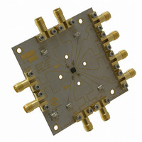
EVAL BOARD FOR NB7L14MMN
Manufacturer
ON Semiconductor
Datasheet
1.NB7L14MMNR2G.pdf
(11 pages)
Specifications of NB7L14MMNEVB
Main Purpose
Timing, Clock Buffer / Driver / Receiver / Translator
Embedded
No
Utilized Ic / Part
NB7L14M
Primary Attributes
Input Up To 12Gb/s & 8GHz
Secondary Attributes
Differential CML Output
Lead Free Status / RoHS Status
Lead free / RoHS Compliant
Other names
NB7L14MMNEVBOS


1. In the differential configuration when the input termination pins (V
2. CML outputs require 50 W receiver termination resistors to V
Table 1. PIN DESCRIPTION
5,16
8,13
Pin
and if no signal is applied on CLK and CLK, then the device will be susceptible to self−oscillation.
10
11
12
14
15
1
2
3
4
6
7
9
−
Name
V
V
CLK
CLK
V
V
TCLK
TCLK
Q3
Q3
Q2
Q2
Q1
Q1
Q0
Q0
EP
CC
EE
LVCMOS, LVTTL,
LVCMOS, LVTTL,
LVPECL, CML,
LVPECL, CML,
Power Supply
Power Supply
CML Output
CML Output
CML Output
CML Output
CML Output
CML Output
CML Output
CML Output
LVDS
LVDS
I/O
−
−
−
V
V
TCLK
TCLK
CLK
CLK
Internal 50 W Termination Pin for CLK.
Inverted Differential Clock/Data Input. (Note 1)
Non−inverted Differential Clock/Data Input. (Note 1)
Internal 50 W Termination Pin for CLK.
Negative Supply Voltage. All V
guarantee proper operation.
Inverted Differential Output 3 with Internal 50 W Source Termination Resistor. (Note 2)
Non−inverted Differential Output 3 with Internal 50 W Source Termination Resistor. (Note 2)
Positive Supply Voltage. All V
guarantee proper operation.
Inverted Differential Output 2 with Internal 50 W Source Termination Resistor. (Note 2)
Non−inverted Differential Output 2 with Internal 50 W Source Termination Resistor. (Note 2)
Inverted Differential Output 1 with Internal 50 W Source Termination Resistor. (Note 2)
Non−inverted Differential Output 1 with Internal 50 W Source Termination Resistor. (Note 2)
Inverted Differential Output 0 with Internal 50 W Source Termination Resistor. (Note 2)
Non−inverted Differential Output 0 with Internal 50 W Source Termination Resistor. (Note 2)
Exposed Pad. Thermal pad on the package bottom must be attached to a heatsinking
conduit to improve heat transfer. It is recommended to connect the EP to the lower
potential (V
Figure 2. QFN−16 Pinout (Top View)
1
2
3
4
V
V
16
EE
5
EE
EE
http://onsemi.com
).
Q0
NB7L14M
15
Q3
6
CC
for proper operation.
TCLK
Q0
14
Q3
2
7
, V
V
V
TCLK
13
8
CC
CC
CC
EE
) are connected to a common termination voltage or left open,
pins must be externally connected to a Power Supply to
Exposed Pad (EP)
pins must be externally connected to a Power Supply to
12
11
10
9
Description
Q1
Q1
Q2
Q2
Related parts for NB7L14MMNEVB
Image
Part Number
Description
Manufacturer
Datasheet
Request
R

Part Number:
Description:
2.5v/3.3vdifferential 1 4 Clock/data Fanout Buffer/translator With Cml Outputs And Internal Termination
Manufacturer:
ON Semiconductor
Datasheet:
Part Number:
Description:
ON Semiconductor [VOLTAGE REGULATOR]
Manufacturer:
ON Semiconductor
Datasheet:
Part Number:
Description:
357-036-542-201 CARDEDGE 36POS DL .156 BLK LOPRO
Manufacturer:
ON Semiconductor
Datasheet:
Part Number:
Description:
357-036-542-201 CARDEDGE 36POS DL .156 BLK LOPRO
Manufacturer:
ON Semiconductor
Datasheet:
Part Number:
Description:
357-036-542-201 CARDEDGE 36POS DL .156 BLK LOPRO
Manufacturer:
ON Semiconductor
Datasheet:
Part Number:
Description:
357-036-542-201 CARDEDGE 36POS DL .156 BLK LOPRO
Manufacturer:
ON Semiconductor
Datasheet:
Part Number:
Description:
357-036-542-201 CARDEDGE 36POS DL .156 BLK LOPRO
Manufacturer:
ON Semiconductor
Datasheet:
Part Number:
Description:
357-036-542-201 CARDEDGE 36POS DL .156 BLK LOPRO
Manufacturer:
ON Semiconductor
Datasheet:
Part Number:
Description:
357-036-542-201 CARDEDGE 36POS DL .156 BLK LOPRO
Manufacturer:
ON Semiconductor
Datasheet:
Part Number:
Description:
357-036-542-201 CARDEDGE 36POS DL .156 BLK LOPRO
Manufacturer:
ON Semiconductor
Datasheet:
Part Number:
Description:
357-036-542-201 CARDEDGE 36POS DL .156 BLK LOPRO
Manufacturer:
ON Semiconductor
Datasheet:
Part Number:
Description:
357-036-542-201 CARDEDGE 36POS DL .156 BLK LOPRO
Manufacturer:
ON Semiconductor
Datasheet:
Part Number:
Description:
Manufacturer:
ON Semiconductor
Datasheet:
Part Number:
Description:
Manufacturer:
ON Semiconductor
Datasheet: