NB7L14MMNEVB ON Semiconductor, NB7L14MMNEVB Datasheet - Page 9
NB7L14MMNEVB
Manufacturer Part Number
NB7L14MMNEVB
Description
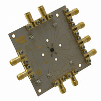
EVAL BOARD FOR NB7L14MMN
Manufacturer
ON Semiconductor
Datasheet
1.NB7L14MMNR2G.pdf
(11 pages)
Specifications of NB7L14MMNEVB
Main Purpose
Timing, Clock Buffer / Driver / Receiver / Translator
Embedded
No
Utilized Ic / Part
NB7L14M
Primary Attributes
Input Up To 12Gb/s & 8GHz
Secondary Attributes
Differential CML Output
Lead Free Status / RoHS Status
Lead free / RoHS Compliant
Other names
NB7L14MMNEVBOS


Application Information
LVCMOS and LVDS signal levels. The limitations for
differential input signal (LVDS, PECL, or CML) are
Recommended R
All NB7L14M inputs can accept PECL, CML, LVTTL,
5.0 V 290 W
3.3 V 150 W
2.5 V 80 W
V
CC
R
T
T
Values
PECL
Driver
V
V
V
50 W
EE
V
CC
CC
EE
CML Driver
Figure 16. PECL to CML Receiver Interface
50 W
R
V
Figure 15. CML to CML Interface
T
EE
Q
R
Q
T
50 W
50 W
http://onsemi.com
9
Z
Z
Z
Z
minimum input swing of 75 mV and the maximum input
swing of 2500 mV. Within these conditions, the input
voltage can range from V
illustrated below in a 50 W environment (Z = 50 W).
V
V
V
V
CC
CC
Bias
Bias
V
V
V
V
TCLK
TCLK
TCLK
TCLK
CLK
CLK
CLK
CLK
V
V
50 W
50 W
V
V
50 W
50 W
CC
CC
CC
EE
EE
to 1.2 V. Examples interfaces are
NB7L14M
NB7L14M
Related parts for NB7L14MMNEVB
Image
Part Number
Description
Manufacturer
Datasheet
Request
R

Part Number:
Description:
2.5v/3.3vdifferential 1 4 Clock/data Fanout Buffer/translator With Cml Outputs And Internal Termination
Manufacturer:
ON Semiconductor
Datasheet:
Part Number:
Description:
ON Semiconductor [VOLTAGE REGULATOR]
Manufacturer:
ON Semiconductor
Datasheet:
Part Number:
Description:
357-036-542-201 CARDEDGE 36POS DL .156 BLK LOPRO
Manufacturer:
ON Semiconductor
Datasheet:
Part Number:
Description:
357-036-542-201 CARDEDGE 36POS DL .156 BLK LOPRO
Manufacturer:
ON Semiconductor
Datasheet:
Part Number:
Description:
357-036-542-201 CARDEDGE 36POS DL .156 BLK LOPRO
Manufacturer:
ON Semiconductor
Datasheet:
Part Number:
Description:
357-036-542-201 CARDEDGE 36POS DL .156 BLK LOPRO
Manufacturer:
ON Semiconductor
Datasheet:
Part Number:
Description:
357-036-542-201 CARDEDGE 36POS DL .156 BLK LOPRO
Manufacturer:
ON Semiconductor
Datasheet:
Part Number:
Description:
357-036-542-201 CARDEDGE 36POS DL .156 BLK LOPRO
Manufacturer:
ON Semiconductor
Datasheet:
Part Number:
Description:
357-036-542-201 CARDEDGE 36POS DL .156 BLK LOPRO
Manufacturer:
ON Semiconductor
Datasheet:
Part Number:
Description:
357-036-542-201 CARDEDGE 36POS DL .156 BLK LOPRO
Manufacturer:
ON Semiconductor
Datasheet:
Part Number:
Description:
357-036-542-201 CARDEDGE 36POS DL .156 BLK LOPRO
Manufacturer:
ON Semiconductor
Datasheet:
Part Number:
Description:
357-036-542-201 CARDEDGE 36POS DL .156 BLK LOPRO
Manufacturer:
ON Semiconductor
Datasheet:
Part Number:
Description:
Manufacturer:
ON Semiconductor
Datasheet:
Part Number:
Description:
Manufacturer:
ON Semiconductor
Datasheet: