CDB4270 Cirrus Logic Inc, CDB4270 Datasheet - Page 6
CDB4270
Manufacturer Part Number
CDB4270
Description
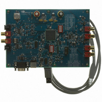
BOARD EVAL FOR CS4270 CODEC
Manufacturer
Cirrus Logic Inc
Datasheet
1.CDB4270.pdf
(50 pages)
Specifications of CDB4270
Main Purpose
Audio, CODEC
Embedded
Yes, FPGA / CPLD
Utilized Ic / Part
CS4270
Primary Attributes
Stereo, 24-Bit, 192 kHz Sample Rate
Secondary Attributes
I²S, S/PDIF Inputs and Outputs, Analog Inputs and Outputs, GUI
Description/function
Audio CODECs
Operating Supply Voltage
5 V
Product
Audio Modules
For Use With/related Products
CS4270
Lead Free Status / RoHS Status
Contains lead / RoHS non-compliant
Lead Free Status / RoHS Status
Lead free / RoHS Compliant, Contains lead / RoHS non-compliant
Other names
598-1002


6
1.7
1.8
1.9
Canned Oscillator
Oscillator Y1 provides a system master clock. This clock is routed through the CS8416 and out of the RMCK
pin when the S/PDIF input is disconnected (refer to the CS8416 data sheet for details on OMCK operation).
To use the canned oscillator as the source of the MCLK signal, remove the S/PDIF input to the CS8416 and
configure the CS8416 appropriately.
The oscillator is mounted in pin sockets, allowing easy removal or replacement. The board is shipped with
a 12.288 MHz crystal oscillator populated at Y1.
External Control Headers
The evaluation board has been designed to allow interfacing with external systems via the J10 and J9 head-
ers.
The 10-pin, 2-row header, J9, allows access to the serial audio signals required to interface with a DSP (see
Figure 71 on page
The 18-pin, 3-row header, J10, allows the user bidirectional access to the SPI
ply removing all of the shunt jumpers from the “NORMAL” position. The user may then choose to connect
a ribbon cable to the “EXTERNAL” position. A single “GND” row for the ribbon cable’s ground connection is
provided to maintain signal integrity. Two unpopulated pull-up resistors are also available should the user
choose to use the CDB for the I²C power rail.
Analog Input
RCA connectors supply the CS4270 analog inputs through passive, AC-coupled, single-ended circuits. A
2 Vrms single-ended signal into the RCA connectors will drive the CS4270 inputs to full scale (1 Vrms). The
input network on the CDB4270 was designed to demonstrate that the CS4270 will provide superior perfor-
mance with up to 2.5 kΩ driving impedances (looking back from the CS4270 inputs) while allowing for
2 Vrms inputs. ADC performance varies depending upon the input impedance of the input network.
Figures 1
impedance.
and
2
show typical THD+N and Dynamic Range performance for the ADC as a function of input
42).
TM
/I²C
®
control signals by sim-
CDB4270
DS686DB3
Related parts for CDB4270
Image
Part Number
Description
Manufacturer
Datasheet
Request
R

Part Number:
Description:
Development Kit
Manufacturer:
Cirrus Logic Inc
Datasheet:
Part Number:
Description:
Development Kit
Manufacturer:
Cirrus Logic Inc
Datasheet:


Part Number:
Description:
High-efficiency PFC + Fluorescent Lamp Driver Reference Design
Manufacturer:
Cirrus Logic Inc
Datasheet:
Part Number:
Description:
Development Kit
Manufacturer:
Cirrus Logic Inc
Datasheet:
Part Number:
Description:
Development Kit
Manufacturer:
Cirrus Logic Inc
Datasheet:

Part Number:
Description:
Development Kit
Manufacturer:
Cirrus Logic Inc
Datasheet:
Part Number:
Description:
Development Kit
Manufacturer:
Cirrus Logic Inc
Datasheet:
Part Number:
Description:
Development Kit
Manufacturer:
Cirrus Logic Inc
Datasheet:
Part Number:
Description:
Development Kit
Manufacturer:
Cirrus Logic Inc
Datasheet:

Part Number:
Description:
EVALUATION BOARD FOR CS8427
Manufacturer:
Cirrus Logic Inc
Datasheet:

Part Number:
Description:
BOARD EVAL FOR CS8416 RCVR
Manufacturer:
Cirrus Logic Inc
Datasheet:

Part Number:
Description:
EVALUATION BOARD FOR CS8420
Manufacturer:
Cirrus Logic Inc
Datasheet:

Part Number:
Description:
KIT DEVELOPMENT EP9315 ARM9
Manufacturer:
Cirrus Logic Inc
Datasheet:

Part Number:
Description:
KIT DEVELOPMENT EP9302 ARM9
Manufacturer:
Cirrus Logic Inc
Datasheet: