AD7940-DBRD Analog Devices Inc, AD7940-DBRD Datasheet - Page 16
AD7940-DBRD
Manufacturer Part Number
AD7940-DBRD
Description
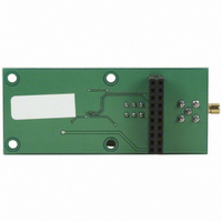
BOARD EVAL FOR AD7940 STAMP SPI
Manufacturer
Analog Devices Inc
Datasheet
1.AD7940BRJZ-REEL7.pdf
(20 pages)
Specifications of AD7940-DBRD
Number Of Adc's
1
Number Of Bits
14
Sampling Rate (per Second)
100k
Data Interface
Serial
Inputs Per Adc
1 Single Ended
Input Range
0 ~ Vdd
Power (typ) @ Conditions
17mW @ 100kSPS & 5 V
Voltage Supply Source
Single Supply
Operating Temperature
-40°C ~ 85°C
Utilized Ic / Part
AD7940
Lead Free Status / RoHS Status
Lead free / RoHS non-compliant


AD7940
SERIAL INTERFACE
Figure 20 shows the detailed timing diagram for serial interfac-
ing to the AD7940. The serial clock provides the conversion
clock and also controls the transfer of information from the
AD7940 during conversion.
The CS signal initiates the data transfer and conversion process.
The falling edge of CS puts the track-and-hold into hold mode,
takes the bus out of three-state, and samples the analog input.
The conversion is also initiated at this point and will require at
least 16 SCLK cycles to complete. Once 15 SCLK falling edges
have elapsed, the track-and-hold will go back into track mode
on the next SCLK rising edge as shown in Figure 20 at Point B.
On the 16th SCLK falling edge, the SDATA line will go back
into three-state. If the rising edge of CS occurs before 16 SCLKs
have elapsed, the conversion will be terminated and the SDATA
line will go back into three-state; otherwise SDATA returns to
three-state on the 16th SCLK falling edge as shown in Figure 20.
Sixteen serial clock cycles are required to perform the conver-
sion process and to access data from the AD7940. CS going low
SDATA
SCLK
CS
3-STATE
t
3
2 LEADING ZEROS
t
2
0
1
ZERO
2
DB13
3
DB12
Figure 20. AD7940 Serial Interface Timing Diagram
4
DB11
t
4
t
6
t
Rev. 0 | Page 16 of 20
CONVERT
5
t
DB10
7
provides the first leading zero to be read in by the microcontroller
or DSP. The remaining data is then clocked out by subsequent
SCLK falling edges beginning with the second leading zero, thus
the first falling clock edge on the serial clock has the first leading
zero provided and also clocks out the second leading zero. The
data transfer will consist of two leading zeros followed by the 14
bits of data. The final bit in the data transfer is valid on the 16th
falling edge, having been clocked out on the previous (15th)
falling edge.
It is also possible to take valid data on each SCLK rising edge
rather than falling edge, since the SCLK cycle time is long
enough to ensure the data is ready on the rising edge of SCLK.
However, the first leading zero will still be driven by the CS
falling edge, and so it can be taken only on the first SCLK falling
edge. It may be ignored, and the first rising edge of SCLK after
the CS falling edge would have the second leading zero pro-
vided and the 15th rising SCLK edge would have DB0 provided.
This method may not work with most microcontrollers/DSPs, but
could possibly be used with FPGAs and ASICs.
13
DB2
14
t
5
DB1
15
B
DB0
16
t
8
3-STATE
t
QUIET
Related parts for AD7940-DBRD
Image
Part Number
Description
Manufacturer
Datasheet
Request
R

Part Number:
Description:
±1.7g Dual-Axis IMEMS Accelerometer Evaluation Board
Manufacturer:
Analog Devices Inc
Datasheet:

Part Number:
Description:
Inertial Sensor Evaluation System
Manufacturer:
Analog Devices Inc
Datasheet:
Part Number:
Description:
Manufacturer:
Analog Devices Inc
Datasheet:
Part Number:
Description:
Manufacturer:
Analog Devices Inc
Datasheet:
Part Number:
Description:
Manufacturer:
Analog Devices Inc
Datasheet:
Part Number:
Description:
Manufacturer:
Analog Devices Inc
Datasheet:
Part Number:
Description:
Manufacturer:
Analog Devices Inc
Datasheet:
Part Number:
Description:
Manufacturer:
Analog Devices Inc
Datasheet:
Part Number:
Description:
Manufacturer:
Analog Devices Inc
Datasheet:
Part Number:
Description:
Manufacturer:
Analog Devices Inc
Datasheet:
Part Number:
Description:
Manufacturer:
Analog Devices Inc
Datasheet:
Part Number:
Description:
Manufacturer:
Analog Devices Inc
Datasheet:
Part Number:
Description:
Manufacturer:
Analog Devices Inc
Datasheet: