AD7940-DBRD Analog Devices Inc, AD7940-DBRD Datasheet - Page 5
AD7940-DBRD
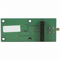
Manufacturer Part Number
AD7940-DBRD
Description
BOARD EVAL FOR AD7940 STAMP SPI
Manufacturer
Analog Devices Inc
Datasheet
1.AD7940BRJZ-REEL7.pdf
(20 pages)
Specifications of AD7940-DBRD
Number Of Adc's
1
Number Of Bits
14
Sampling Rate (per Second)
100k
Data Interface
Serial
Inputs Per Adc
1 Single Ended
Input Range
0 ~ Vdd
Power (typ) @ Conditions
17mW @ 100kSPS & 5 V
Voltage Supply Source
Single Supply
Operating Temperature
-40°C ~ 85°C
Utilized Ic / Part
AD7940
Lead Free Status / RoHS Status
Lead free / RoHS non-compliant


TIMING SPECIFICATIONS
Sample tested at initial release to ensure compliance. All input signals are specified with tr = tf = 5 ns (10% to 90% of V
a voltage level of 1.6 V.
V
Table 3.
Parameter
f
t
t
t
t
t
t
t
t
t
t
t
1
2
3
4
SCLK
CONVERT
QUIET
1
2
3
4
5
6
7
8
POWER-UP
Mark/space ratio for the SCLK input is 40/60 to 60/40.
Measured with the load circuit of
t
back to remove the effects of charging or discharging the 50 pF capacitor. This means that the time, t
time of the part and is independent of the bus loading.
See the
2
2
3
8
DD
is derived form the measured time taken by the data outputs to change 0.5 V when loaded with the circuit of
1
= 2.50 V to 5.5 V; T
4
Power vs. Throughput Rate
A
= T
Figure 2
MIN
3 V
250
2.5
16 × t
50
10
10
48
120
0.4 t
0.4 t
10
45
1
section.
to T
Limit at T
SCLK
SCLK
SCLK
and defined as the time required for the output to cross 0.8 V or 2.0 V.
MAX
, unless otherwise noted.
MIN
5 V
250
2.5
16 × t
50
10
10
35
80
0.4 t
0.4 t
10
35
1
Figure 2. Load Circuit for Digital Output Timing Specification
, T
SCLK
SCLK
MAX
SCLK
TO OUTPUT
PIN
Unit
kHz min
MHz max
min
ns min
ns min
ns min
ns max
ns max
ns min
ns min
ns min
ns max
µs typ
50pF
Rev. 0 | Page 5 of 20
C
L
200µA
200µA
Description
Minimum quiet time required between bus relinquish and start of
next conversion
Minimum CS pulse width
CS to SCLK setup time
Delay from CS until SDATA three-state disabled
Data access time after SCLK falling edge
SCLK low pulse width
SCLK high pulse width
SCLK to data valid hold time
SCLK falling edge to SDATA high impedance
Power up time from full power-down
I
I
OL
OH
1.6V
8
, quoted in the timing characteristics is the true bus relinquish
Figure 2.
The measured number is then extrapolated
DD
) and timed from
AD7940
Related parts for AD7940-DBRD
Image
Part Number
Description
Manufacturer
Datasheet
Request
R

Part Number:
Description:
±1.7g Dual-Axis IMEMS Accelerometer Evaluation Board
Manufacturer:
Analog Devices Inc
Datasheet:

Part Number:
Description:
Inertial Sensor Evaluation System
Manufacturer:
Analog Devices Inc
Datasheet:
Part Number:
Description:
Manufacturer:
Analog Devices Inc
Datasheet:
Part Number:
Description:
Manufacturer:
Analog Devices Inc
Datasheet:
Part Number:
Description:
Manufacturer:
Analog Devices Inc
Datasheet:
Part Number:
Description:
Manufacturer:
Analog Devices Inc
Datasheet:
Part Number:
Description:
Manufacturer:
Analog Devices Inc
Datasheet:
Part Number:
Description:
Manufacturer:
Analog Devices Inc
Datasheet:
Part Number:
Description:
Manufacturer:
Analog Devices Inc
Datasheet:
Part Number:
Description:
Manufacturer:
Analog Devices Inc
Datasheet:
Part Number:
Description:
Manufacturer:
Analog Devices Inc
Datasheet:
Part Number:
Description:
Manufacturer:
Analog Devices Inc
Datasheet:
Part Number:
Description:
Manufacturer:
Analog Devices Inc
Datasheet: