CDB43L21 Cirrus Logic Inc, CDB43L21 Datasheet - Page 11
CDB43L21
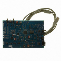
Manufacturer Part Number
CDB43L21
Description
BOARD EVAL FOR CS43L21 DAC
Manufacturer
Cirrus Logic Inc
Datasheet
1.CDB-43L21.pdf
(25 pages)
Specifications of CDB43L21
Description/function
Audio D/A
Operating Supply Voltage
5 V
Product
Audio Modules
For Use With/related Products
CS43L21
Lead Free Status / RoHS Status
Contains lead / RoHS non-compliant
Lead Free Status / RoHS Status
Lead free / RoHS Compliant, Contains lead / RoHS non-compliant
Other names
598-1528


DS723DB1
3. HARDWARE MODE CONTROL
The CDB may be configured without the use of a software control port through the use of two switches, “FPGA H/W
Control” and “CS43L21 H/W Control.” These switches are enabled in Hardware Mode only and ignored in Software
Mode. The CDB43L21 automatically enters Hardware Mode upon initial power up, when exiting Software Mode,
upon termination of the Cirrus FlexGUI software, or by disconnecting the RS-232 serial cable.
3.1
3.2
FPGA H/W Control
The “FPGA H/W Control” switch sets up the CDB in 11 pre-defined routing topologies in Hardware Mode.
The tables and figures below describe each switch setting. The At-A-Glance Controls table provides a quick
reference for all presets.
CS43L21 H/W Control
The stand-alone “CS43L21 H/W Control” switch controls the Hardware Mode options of the CS43L21. A
description of each switch is outlined in the following table:
00 - CS8415 MCLK / CS8415 clocks/data route through FPGA
01 - I/O Header MCLK / I/O Header clocks/data route through FPGA
10 - Oscillator MCLK / I/O Header clocks/data route through FPGA
11 - Reserved
Routing
Figure 4
Figure 5
Figure 6
Figure 7
Figure 8
Signal
DE-EMPHASIS
MCLKDIV2
1
2
3
4
5
Switch
I2S/LJ
M/S
S[3:0]
0000
0100
0110
1000
1010
Oscillator MCLK
CS8415 MCLK
CS8415 Clocks/Data
I/O Clocks/Data
CS43L21 Clocks, I/O Data
I/O Clocks/Data
CS43L21 Clocks, I/O Data
I/O MCLK
Position
General Description
S[3:2]
LO
LO
LO
LO
HI
HI
HI
HI
Table 1. MCLK and Clock/Data Routing Options
LRCK and SCLK are inputs to CS43L21
LRCK and SCLK are outputs to CS43L21
Internal MCLK to CS43L21 not divided
Internal MCLK to CS43L21 divided by 2
CS43L21 Interface Format: Left-Justified
CS43L21 Interface Format: I²S
No internal De-emphasis applied to CS43L21
44.1 kHz internal De-emphasis applied to CS43L21
Table 2. CS43L21 H/W Mode Control
At-A-Glance Controls
1) CS8415 masters MCLK. 2) CS8415 masters PCM clocks.
3) CS8415 data into SDIN.
1) I/O masters MCLK. 2) I/O masters PCM clocks.
3) I/O data into SDIN.
1) I/O masters MCLK. 2) CS43L21 masters PCM clocks.
3) I/O data into SDIN.
1) Oscillator masters MCLK. 2) I/O masters PCM clocks.
3) I/O data into SDIN.
1) Oscillator masters MCLK. 2) CS43L21 masters PCM
clocks.
3) I/O data into SDIN.
1 - CS43L21 Master Routing
0 - CS43L21 Slave Routing
Function
S[1]
Detailed Description
0 - Normal Operation
1 - Reserved
CDB43L21
S[0]
11
Related parts for CDB43L21
Image
Part Number
Description
Manufacturer
Datasheet
Request
R

Part Number:
Description:
EVAL BOARD FOR CS43L21
Manufacturer:
Cirrus Logic Inc
Datasheet:

Part Number:
Description:
Development Kit
Manufacturer:
Cirrus Logic Inc
Datasheet:
Part Number:
Description:
Development Kit
Manufacturer:
Cirrus Logic Inc
Datasheet:


Part Number:
Description:
High-efficiency PFC + Fluorescent Lamp Driver Reference Design
Manufacturer:
Cirrus Logic Inc
Datasheet:
Part Number:
Description:
Development Kit
Manufacturer:
Cirrus Logic Inc
Datasheet:
Part Number:
Description:
Development Kit
Manufacturer:
Cirrus Logic Inc
Datasheet:

Part Number:
Description:
Development Kit
Manufacturer:
Cirrus Logic Inc
Datasheet:
Part Number:
Description:
Development Kit
Manufacturer:
Cirrus Logic Inc
Datasheet:
Part Number:
Description:
Development Kit
Manufacturer:
Cirrus Logic Inc
Datasheet:

Part Number:
Description:
EVALUATION BOARD FOR CS8427
Manufacturer:
Cirrus Logic Inc
Datasheet:

Part Number:
Description:
BOARD EVAL FOR CS8416 RCVR
Manufacturer:
Cirrus Logic Inc
Datasheet:

Part Number:
Description:
EVALUATION BOARD FOR CS8420
Manufacturer:
Cirrus Logic Inc
Datasheet:

Part Number:
Description:
KIT DEVELOPMENT EP9315 ARM9
Manufacturer:
Cirrus Logic Inc
Datasheet:

Part Number:
Description:
KIT DEVELOPMENT EP9302 ARM9
Manufacturer:
Cirrus Logic Inc
Datasheet: