CDB43L21 Cirrus Logic Inc, CDB43L21 Datasheet - Page 14
CDB43L21
Manufacturer Part Number
CDB43L21
Description
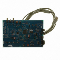
BOARD EVAL FOR CS43L21 DAC
Manufacturer
Cirrus Logic Inc
Datasheet
1.CDB-43L21.pdf
(25 pages)
Specifications of CDB43L21
Description/function
Audio D/A
Operating Supply Voltage
5 V
Product
Audio Modules
For Use With/related Products
CS43L21
Lead Free Status / RoHS Status
Contains lead / RoHS non-compliant
Lead Free Status / RoHS Status
Lead free / RoHS Compliant, Contains lead / RoHS non-compliant
Other names
598-1528


14
4. SYSTEM CONNECTIONS
5. JUMPER SETTINGS
H/W BOARD RESET
*Default factory settings
Notes:
S/PDIF OPTICAL IN
FPGA PROGRAM
JMP
S/PDIF COAX IN
Headphone Jack
CONNECTOR
S/W CONTROL
J31
J36
J25
J28
J52
J48
J47
J53
J10
J13
MICRO RESET
J6
J4
MICRO JTAG
SPEAKER +
FPGA JTAG
SPEAKER -
I/O Header
RS232
RIGHT
LEFT
GND
USB
+5V
HP LOAD
HP LOAD
LABEL
+VA_HP
Channel
Channel
16 ohm
16 ohm
VA_HP
Right
1. Refer to
Left
VA
VD
VA
VD
VL
VL
Selects source of voltage for
Selects source of voltage for
Selects source of voltage for
Selects source of voltage for
Selects between filtered and
Selects between filtered and
the VL supply *
OPT1
Current Measurement
REF
J109
J110
Section 9 on page 25
J26
J27
J95
J94
J61
J78
J19
J20
J72
J73
J11
S4
S2
S1
J5
the VA_HP supply
non-filtered output
non-filtered output
Load Simulation
Load Simulation
the VD supply
the VA supply
PURPOSE
INPUT/OUTPUT
Input/Output
Input/Output
Input/Output
Input/Output
Input/Output
Input/Output
(Note 1)
Output
Output
Output
Input
Input
Input
Input
Input
Input
Input
Table 3. System Connections
Table 4. Jumper Settings
regarding jumper settings for J31.
AOUTA (LPF) Connects low-pass filtered AOUTA to LEFT RCA jack
AOUTB (LPF) Connects lowpass filtered AOUTA to RIGHT RCA jack
POSITION
*SHUNTED 1 Ω series resistor is shorted
SHUNTED
SHUNTED
*Not con-
*Not con-
*AOUTB
*AOUTA
*+1.8 V
*+1.8 V
*+1.8 V
*+1.8 V
+2.5 V
+3.3 V
+2.5 V
+2.5 V
+2.5 V
nected
nected
OPEN
+5.0 V Power Supply
Ground Reference
Serial connection to PC for SPI / I²C control port signals
USB connection to PC for SPI / I²C control port signals
CS8415 digital audio input via optical cable
CS8415 digital audio input via coaxial cable
I/O for Clocks & Data
I/O for external SPI / I²C control port signals
I/O for programming the micro controller (U84)
I/O for programming the FPGA (U14)
Reset for the micro controller (U84)
Reload Xilinx Flash program into the FPGA (U14)
Reset for the CS43L21 (U1)
RCA phono jacks for analog outputs
Binding Post connected to LM4889 speaker driver for analog out-
puts
Headphone jack for analog outputs
Voltage source is +1.8 V regulator
Voltage source is +2.5 V regulator
Voltage source is +3.3 V regulator
Voltage source is +1.8 V regulator
Voltage source is +2.5 V regulator
Voltage source is +1.8 V regulator
Voltage source is +2.5 V regulator
Voltage source is +1.8 V regulator
Voltage source is +2.5 V regulator
1 Ω series resistor in power supply path
Connects AOUTA of part directly to LEFT RCA jack
Connects AOUTB of part directly to RIGHT RCA jack
16 Ω resistor shunted from AOUTA to GND
Jumper placed on pin 1
16 Ω resistor shunted from AOUTB to GND
Jumper placed on pin 1
SIGNAL PRESENT
FUNCTION SELECTED
CDB43L21
DS723DB1
Related parts for CDB43L21
Image
Part Number
Description
Manufacturer
Datasheet
Request
R

Part Number:
Description:
EVAL BOARD FOR CS43L21
Manufacturer:
Cirrus Logic Inc
Datasheet:

Part Number:
Description:
Development Kit
Manufacturer:
Cirrus Logic Inc
Datasheet:
Part Number:
Description:
Development Kit
Manufacturer:
Cirrus Logic Inc
Datasheet:


Part Number:
Description:
High-efficiency PFC + Fluorescent Lamp Driver Reference Design
Manufacturer:
Cirrus Logic Inc
Datasheet:
Part Number:
Description:
Development Kit
Manufacturer:
Cirrus Logic Inc
Datasheet:
Part Number:
Description:
Development Kit
Manufacturer:
Cirrus Logic Inc
Datasheet:

Part Number:
Description:
Development Kit
Manufacturer:
Cirrus Logic Inc
Datasheet:
Part Number:
Description:
Development Kit
Manufacturer:
Cirrus Logic Inc
Datasheet:
Part Number:
Description:
Development Kit
Manufacturer:
Cirrus Logic Inc
Datasheet:

Part Number:
Description:
EVALUATION BOARD FOR CS8427
Manufacturer:
Cirrus Logic Inc
Datasheet:

Part Number:
Description:
BOARD EVAL FOR CS8416 RCVR
Manufacturer:
Cirrus Logic Inc
Datasheet:

Part Number:
Description:
EVALUATION BOARD FOR CS8420
Manufacturer:
Cirrus Logic Inc
Datasheet:

Part Number:
Description:
KIT DEVELOPMENT EP9315 ARM9
Manufacturer:
Cirrus Logic Inc
Datasheet:

Part Number:
Description:
KIT DEVELOPMENT EP9302 ARM9
Manufacturer:
Cirrus Logic Inc
Datasheet: