CDB43L21 Cirrus Logic Inc, CDB43L21 Datasheet - Page 4
CDB43L21
Manufacturer Part Number
CDB43L21
Description
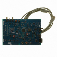
BOARD EVAL FOR CS43L21 DAC
Manufacturer
Cirrus Logic Inc
Datasheet
1.CDB-43L21.pdf
(25 pages)
Specifications of CDB43L21
Description/function
Audio D/A
Operating Supply Voltage
5 V
Product
Audio Modules
For Use With/related Products
CS43L21
Lead Free Status / RoHS Status
Contains lead / RoHS non-compliant
Lead Free Status / RoHS Status
Lead free / RoHS Compliant, Contains lead / RoHS non-compliant
Other names
598-1528


4
1. SYSTEM OVERVIEW
The CDB43L21 evaluation board is an excellent means for evaluating the CS43L21. Digital audio signal interfaces
are provided, and an FPGA is used for easily configuring the board.
and
The CDB43L21 schematic set has been partitioned into six pages and is shown in
Connections” on page 14
settings for all jumpers.
1.1
1.2
1.3
1.4
WARNING: Please refer to the CS43L21 data sheet for allowable voltage levels.
Section 3. “Hardware Mode Control” on page 11
Power
Power is supplied to the evaluation board through the +5.0 V binding posts. Jumpers connect the
CS43L21’s power supplies to a regulated voltage of +1.8 V, 2.5 V or +3.3 V for VL and +1.8 V or 2.5 V for
VD, VA and VA_HP. All voltage inputs must be referenced to the black binding post ground connector.
For current measurement purposes only, a series resistor is connected to each supply. The current is easily
calculated by measuring the voltage drop across this resistor.
NOTE: The stake headers connected in parallel with these resistors must be shunted with the supplied
jumper during normal operation.
Grounding and Power Supply Decoupling
The CS43L21 requires careful attention to power supply and grounding arrangements to optimize perfor-
mance. The CDB43L21 demonstrates these optimal arrangements.
view of the connections to the CS43L21.
on page 23
pacitors are located as close to the CS43L21 as possible. Extensive use of ground plane fill in the evaluation
board yields large reductions in radiated noise.
FPGA
The FPGA provides digital signal routing between the CS43L21, CS8415 and the I/O stake header. It also
configures the Hardware Mode options of the CS8415 and provides routing control of the system master
clock from an on-board oscillator, the CS8415 and the I/O stake header. The Cirrus FlexGUI software and
“FPGA H/W Control” switches provide full control of the FPGA’s routing and configuration options.
Section 2. “Software Mode Control” on page 7
configuration details.
CS43L21
A complete description of the CS43L21 is included in the CS43L21 product data sheet, and a schematic is
provided in
The CS43L21 may be configured using either the Cirrus FlexGUI or the on-board “CS43L21 H/W Control”
switches. The Software Mode control port registers are accessible through the “Register Maps” tab of the
Cirrus FlexGUI software. This tab provides low-level control of each bit. For easier configuration, additional
tabs provide high-level control. The Hardware Mode, stand-alone controls for the CS43L21 are accessible
through the on-board, stand-alone switches, “CS43L21 H/W Control.”
Clock and data source selections are made in the control port of the FPGA, accessible through the “General
Configurations” tab of the Cirrus FlexGUI software or through the on-board “FPGA H/W Control” switches.
Figure 10 on page
shows the top layout, and
provides a description of all stake headers and connectors, including the default factory
16.
Figure 18 on page 24
Figure 16 on page 22
provide configuration details.
and
Section 3. “Hardware Mode Control” on page 11
Section 2. “Software Mode Control” on page 7
shows the bottom layout. The decoupling ca-
shows the component placement,
Figure 9 on page 15
Figures 10
through 15.
provides an over-
CDB43L21
DS723DB1
Figure 17
“System
provide
Related parts for CDB43L21
Image
Part Number
Description
Manufacturer
Datasheet
Request
R

Part Number:
Description:
EVAL BOARD FOR CS43L21
Manufacturer:
Cirrus Logic Inc
Datasheet:

Part Number:
Description:
Development Kit
Manufacturer:
Cirrus Logic Inc
Datasheet:
Part Number:
Description:
Development Kit
Manufacturer:
Cirrus Logic Inc
Datasheet:


Part Number:
Description:
High-efficiency PFC + Fluorescent Lamp Driver Reference Design
Manufacturer:
Cirrus Logic Inc
Datasheet:
Part Number:
Description:
Development Kit
Manufacturer:
Cirrus Logic Inc
Datasheet:
Part Number:
Description:
Development Kit
Manufacturer:
Cirrus Logic Inc
Datasheet:

Part Number:
Description:
Development Kit
Manufacturer:
Cirrus Logic Inc
Datasheet:
Part Number:
Description:
Development Kit
Manufacturer:
Cirrus Logic Inc
Datasheet:
Part Number:
Description:
Development Kit
Manufacturer:
Cirrus Logic Inc
Datasheet:

Part Number:
Description:
EVALUATION BOARD FOR CS8427
Manufacturer:
Cirrus Logic Inc
Datasheet:

Part Number:
Description:
BOARD EVAL FOR CS8416 RCVR
Manufacturer:
Cirrus Logic Inc
Datasheet:

Part Number:
Description:
EVALUATION BOARD FOR CS8420
Manufacturer:
Cirrus Logic Inc
Datasheet:

Part Number:
Description:
KIT DEVELOPMENT EP9315 ARM9
Manufacturer:
Cirrus Logic Inc
Datasheet:

Part Number:
Description:
KIT DEVELOPMENT EP9302 ARM9
Manufacturer:
Cirrus Logic Inc
Datasheet: