NCP3065D3SLDGEVB ON Semiconductor, NCP3065D3SLDGEVB Datasheet - Page 2
NCP3065D3SLDGEVB
Manufacturer Part Number
NCP3065D3SLDGEVB
Description
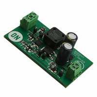
EVAL BOARD FOR NCP3065D3SLDG
Manufacturer
ON Semiconductor
Datasheets
1.NCP3065DR2G.pdf
(18 pages)
2.NCP3065D3SLDGEVB.pdf
(1 pages)
3.NCP3065D3SLDGEVB.pdf
(11 pages)
Specifications of NCP3065D3SLDGEVB
Design Resources
NCP3065D3SLDGEVB BOM NCP3065D3SLDGEVB Gerber Files NCP3065D3SLDGEVB Schematic
Current - Output / Channel
700mA
Outputs And Type
1, Non-Isolated
Voltage - Output
7 ~ 23 V
Voltage - Input
12V
Utilized Ic / Part
NCP3065
Core Chip
NCP3065
Topology
SEPIC
No. Of Outputs
1
Output Current
1A
Output Voltage
23V
Dimming Control Type
PWM
Development Tool Type
Hardware - Eval/Demo Board
Leaded Process Compatible
Yes
Rohs Compliant
Yes
Lead Free Status / RoHS Status
Lead free / RoHS Compliant
Features
-
Lead Free Status / Rohs Status
Lead free / RoHS Compliant
For Use With/related Products
NCP3065D3SLDG
Other names
NCP3065D3SLDGEVBOS


November 2007, Rev.2
Schematic
Design Notes
voltage range can overlap the output voltage range. The basic schematic is shown in Figure 2.
connected in parallel to L2, and energy from CP is transferred to L2. The voltage across L2 is the
same as the CP voltage, which is the same as the input voltage. At this time, the diode is reverse
biased and COUT supplies output current.
and COUT. This current recharges CP for the next cycle. Current from L2 also flows through D1 to
the load and COUT that is recharging for the next cycle.
coupled. Another advantage is that if coupled inductors are used there is very small input current
ripple.
A SEPIC (single-ended primary inductance converter) is distinguished by the fact that its input
When switch SW is ON, energy from the input is stored in inductor L1. Capacitor CP is
If the switch SW is OFF, current in L1 flows through CP and D1 then continues to the load
Inductors L1 and L2 could be uncoupled, but then they must be twice as large as if they are
Values of coupled inductors are set by these equations:
where r is the maximum inductor current ripple factor.
L
Figure 2 – Generalized SEPIC schematic
Δ
1
2 ,
Figure 1 – SEPIC converter schematic
I
D
=
=
r
V
=
⋅
IN
2
V
I
⋅
OUT
OUT
min
f
Δ ⋅
V
1
min
⋅
OUT
−
I
D
D
www.onsemi.com
D
DN06031/D
+
min
=
V
=
2
IN
0
⋅
8 .
min
250
⋅
8
0
⋅
7 .
⋅
. 0
=
10
⋅
47
7
1
3
2 .
7
−
⋅
. 0
. 0
2 .
+
. 0
47
51
8
47
=
=
=
. 0
15
. 0
47
0 .
51
μ
A
H
2
Related parts for NCP3065D3SLDGEVB
Image
Part Number
Description
Manufacturer
Datasheet
Request
R

Part Number:
Description:
Up to 1.5 A Constant Current Switching Regulator for LEDs
Manufacturer:
ON Semiconductor
Datasheet:

Part Number:
Description:
EVAL BOARD FOR NCP3065SOBCKG
Manufacturer:
ON Semiconductor
Datasheet:

Part Number:
Description:
EVAL BOARD FOR NCP3065SOBSTG
Manufacturer:
ON Semiconductor
Datasheet:

Part Number:
Description:
EVAL BOARD FOR NCP30653ABCKG
Manufacturer:
ON Semiconductor
Datasheet:
Part Number:
Description:
ON Semiconductor [VOLTAGE REGULATOR]
Manufacturer:
ON Semiconductor
Datasheet:
Part Number:
Description:
357-036-542-201 CARDEDGE 36POS DL .156 BLK LOPRO
Manufacturer:
ON Semiconductor
Datasheet:
Part Number:
Description:
357-036-542-201 CARDEDGE 36POS DL .156 BLK LOPRO
Manufacturer:
ON Semiconductor
Datasheet:
Part Number:
Description:
357-036-542-201 CARDEDGE 36POS DL .156 BLK LOPRO
Manufacturer:
ON Semiconductor
Datasheet:
Part Number:
Description:
357-036-542-201 CARDEDGE 36POS DL .156 BLK LOPRO
Manufacturer:
ON Semiconductor
Datasheet:
Part Number:
Description:
357-036-542-201 CARDEDGE 36POS DL .156 BLK LOPRO
Manufacturer:
ON Semiconductor
Datasheet:
Part Number:
Description:
357-036-542-201 CARDEDGE 36POS DL .156 BLK LOPRO
Manufacturer:
ON Semiconductor
Datasheet:
Part Number:
Description:
357-036-542-201 CARDEDGE 36POS DL .156 BLK LOPRO
Manufacturer:
ON Semiconductor
Datasheet:
Part Number:
Description:
357-036-542-201 CARDEDGE 36POS DL .156 BLK LOPRO
Manufacturer:
ON Semiconductor
Datasheet:
Part Number:
Description:
357-036-542-201 CARDEDGE 36POS DL .156 BLK LOPRO
Manufacturer:
ON Semiconductor
Datasheet:
Part Number:
Description:
357-036-542-201 CARDEDGE 36POS DL .156 BLK LOPRO
Manufacturer:
ON Semiconductor
Datasheet: