NCP3065D3SLDGEVB ON Semiconductor, NCP3065D3SLDGEVB Datasheet - Page 4
NCP3065D3SLDGEVB
Manufacturer Part Number
NCP3065D3SLDGEVB
Description
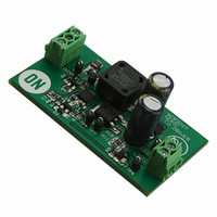
EVAL BOARD FOR NCP3065D3SLDG
Manufacturer
ON Semiconductor
Datasheets
1.NCP3065DR2G.pdf
(18 pages)
2.NCP3065D3SLDGEVB.pdf
(1 pages)
3.NCP3065D3SLDGEVB.pdf
(11 pages)
Specifications of NCP3065D3SLDGEVB
Design Resources
NCP3065D3SLDGEVB BOM NCP3065D3SLDGEVB Gerber Files NCP3065D3SLDGEVB Schematic
Current - Output / Channel
700mA
Outputs And Type
1, Non-Isolated
Voltage - Output
7 ~ 23 V
Voltage - Input
12V
Utilized Ic / Part
NCP3065
Core Chip
NCP3065
Topology
SEPIC
No. Of Outputs
1
Output Current
1A
Output Voltage
23V
Dimming Control Type
PWM
Development Tool Type
Hardware - Eval/Demo Board
Leaded Process Compatible
Yes
Rohs Compliant
Yes
Lead Free Status / RoHS Status
Lead free / RoHS Compliant
Features
-
Lead Free Status / Rohs Status
Lead free / RoHS Compliant
For Use With/related Products
NCP3065D3SLDG
Other names
NCP3065D3SLDGEVBOS


November 2007, Rev.2
function at low duty cycle.
and output voltage range. If this circuit is used for specified load only, it should be tuned by this
resistor to better efficiency and line regulation.
dimming frequency is about 200 Hz. For frequencies below 100 Hz the human eye will see the
flicker. The dimming function utilizes the NCP3065’s peak current protection input. The second way
to achieve this is to use the FB pin. See figure 10.
Conclusion
supply with wide input range (8-20V). The advantages of this circuit include its small size, low price,
wide input and output voltage ranges, and very small input current ripple.
and with current
The C4 coupling capacitor is selected based on input voltage and on current
and its minimal value is
The output capacitor’s current is
The value could be much larger for higher stability, but a higher value impacts the dimming
The resistor R8 is used to stabilize feedback loop. Used value is compromise for whole input
X1-3 input is used for dimming. The dimming signal level is 2-10 V. The recommended
This circuit is ideal in applications with strings of two to six LED chips powered from a power
I
C
C
4
5
RMS
>
C
I
V
=
4
V
D
C
OUT
5
V
>
IN
max
=
OUT
. 0
min
f
V
min
I
V
⋅
05
I
D
OUT
r
IN
⋅
OUT
1
=
max
I
⋅
⋅
V
OUT
⋅
V
V
⋅
I
OUT
⋅
OUT
IN
OUT
=
D
1
min
V
I
min
−
min
V
www.onsemi.com
D
D
max
1
IN
⋅
DN06031/D
1
OUT
−
D
D
D
max
⋅
+
=
D
max
min
f
max
V
+
I
max
max
OUT
OUT
V
=
IN
. 0
=
=
=
=
min
05
250
=
0
18
0
0
7 .
7
⋅
7 .
23
7 .
8
8
3 .
+
=
⋅
A
⋅
10
⋅
1
⋅
8
⋅
250
23
. 0
0
23
−
0
. 0
3
7 .
47
7 .
23
. 0
=
74
⋅
+
⋅
0
⋅
74
10
41
. 0
8
1 .
1
47
V
⋅
=
−
3
. 0
=
7
. 0
=
. 0
74
3 .
1
74
2 .
74
2
=
μ
A
1
F
=
7 .
1
μ
2 .
F
A
4
Related parts for NCP3065D3SLDGEVB
Image
Part Number
Description
Manufacturer
Datasheet
Request
R

Part Number:
Description:
Up to 1.5 A Constant Current Switching Regulator for LEDs
Manufacturer:
ON Semiconductor
Datasheet:

Part Number:
Description:
EVAL BOARD FOR NCP3065SOBCKG
Manufacturer:
ON Semiconductor
Datasheet:

Part Number:
Description:
EVAL BOARD FOR NCP3065SOBSTG
Manufacturer:
ON Semiconductor
Datasheet:

Part Number:
Description:
EVAL BOARD FOR NCP30653ABCKG
Manufacturer:
ON Semiconductor
Datasheet:
Part Number:
Description:
ON Semiconductor [VOLTAGE REGULATOR]
Manufacturer:
ON Semiconductor
Datasheet:
Part Number:
Description:
357-036-542-201 CARDEDGE 36POS DL .156 BLK LOPRO
Manufacturer:
ON Semiconductor
Datasheet:
Part Number:
Description:
357-036-542-201 CARDEDGE 36POS DL .156 BLK LOPRO
Manufacturer:
ON Semiconductor
Datasheet:
Part Number:
Description:
357-036-542-201 CARDEDGE 36POS DL .156 BLK LOPRO
Manufacturer:
ON Semiconductor
Datasheet:
Part Number:
Description:
357-036-542-201 CARDEDGE 36POS DL .156 BLK LOPRO
Manufacturer:
ON Semiconductor
Datasheet:
Part Number:
Description:
357-036-542-201 CARDEDGE 36POS DL .156 BLK LOPRO
Manufacturer:
ON Semiconductor
Datasheet:
Part Number:
Description:
357-036-542-201 CARDEDGE 36POS DL .156 BLK LOPRO
Manufacturer:
ON Semiconductor
Datasheet:
Part Number:
Description:
357-036-542-201 CARDEDGE 36POS DL .156 BLK LOPRO
Manufacturer:
ON Semiconductor
Datasheet:
Part Number:
Description:
357-036-542-201 CARDEDGE 36POS DL .156 BLK LOPRO
Manufacturer:
ON Semiconductor
Datasheet:
Part Number:
Description:
357-036-542-201 CARDEDGE 36POS DL .156 BLK LOPRO
Manufacturer:
ON Semiconductor
Datasheet:
Part Number:
Description:
357-036-542-201 CARDEDGE 36POS DL .156 BLK LOPRO
Manufacturer:
ON Semiconductor
Datasheet: