NCP3065SOBSTGEVB ON Semiconductor, NCP3065SOBSTGEVB Datasheet - Page 14
NCP3065SOBSTGEVB
Manufacturer Part Number
NCP3065SOBSTGEVB
Description
EVAL BOARD FOR NCP3065SOBSTG
Manufacturer
ON Semiconductor
Datasheets
1.NCP3065DR2G.pdf
(18 pages)
2.NCP3065SOBSTGEVB.pdf
(1 pages)
3.NCP3065SOBSTGEVB.pdf
(18 pages)
Specifications of NCP3065SOBSTGEVB
Design Resources
NCP3065 Boost Eval Board BOM NCP3065SOBSTGEVB Gerber Files NCP3065 Boost Eval Board Schematic
Current - Output / Channel
350mA
Outputs And Type
1, Non-Isolated
Voltage - Output
20 V
Voltage - Input
12V
Utilized Ic / Part
NCP3065
Core Chip
NCP3065
Topology
Buck-Boost
No. Of Outputs
1
Dimming Control Type
PWM
Development Tool Type
Hardware - Eval/Demo Board
Leaded Process Compatible
Yes
Mcu Supported Families
NCP3065
Rohs Compliant
Yes
Lead Free Status / RoHS Status
Lead free / RoHS Compliant
Features
-
Lead Free Status / Rohs Status
Lead free / RoHS Compliant
For Use With/related Products
NCP3065SOBSTG
Other names
NCP3065SOBSTGEVBOS


Figure 20. Switching Waveform With Pulse Feedback
Figure 19.
LED
Oscillator
Switching Waveform Without Pulse
V
SENSE
V
Feedback
ref
Current Comparator
Output from Peak
+
−
Figure 18. Burst−Mode Architecture
http://onsemi.com
14
resistor on the switching waveforms and load current ripple.
This results in a fixed frequency switching with constant
duty cycle, which is only dependent upon the input and
output voltage ratio. When the ratio (V
(high duty cycle) over the entire input voltage range, the
pulse feedback is not needed.
Boost Converter Topology
When the low side power switch is turned on, current drawn
from the input begins to flow through the inductor and the
current I
the current I
capacitor and load. At the same time the inductor voltage is
added with the input power supply voltage and as long as this
is higher than the output voltage, the current continues to
flow through the diode. Provided that the current through the
inductor is always positive, the converter is operating in
continuous conduction mode (CCM). On the next switching
cycle, the process is repeated.
Figures 19 and 20 show the effect of the pulse feedback
The Boost converter schematic is illustrated in Figure 22.
ton
rises up. When the low side switch is turned off,
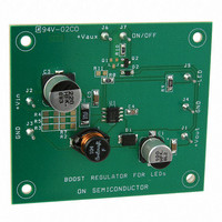
Boost Converter Demo Board
toff
Figure 21. Boost Demo Board
circulates through diode D1 to the output
OUT
/V
IN
) is near 1
Related parts for NCP3065SOBSTGEVB
Image
Part Number
Description
Manufacturer
Datasheet
Request
R

Part Number:
Description:
Up to 1.5 A Constant Current Switching Regulator for LEDs
Manufacturer:
ON Semiconductor
Datasheet:

Part Number:
Description:
EVAL BOARD FOR NCP3065SOBCKG
Manufacturer:
ON Semiconductor
Datasheet:

Part Number:
Description:
EVAL BOARD FOR NCP30653ABCKG
Manufacturer:
ON Semiconductor
Datasheet:
Part Number:
Description:
ON Semiconductor [VOLTAGE REGULATOR]
Manufacturer:
ON Semiconductor
Datasheet:
Part Number:
Description:
357-036-542-201 CARDEDGE 36POS DL .156 BLK LOPRO
Manufacturer:
ON Semiconductor
Datasheet:
Part Number:
Description:
357-036-542-201 CARDEDGE 36POS DL .156 BLK LOPRO
Manufacturer:
ON Semiconductor
Datasheet:
Part Number:
Description:
357-036-542-201 CARDEDGE 36POS DL .156 BLK LOPRO
Manufacturer:
ON Semiconductor
Datasheet:
Part Number:
Description:
357-036-542-201 CARDEDGE 36POS DL .156 BLK LOPRO
Manufacturer:
ON Semiconductor
Datasheet:
Part Number:
Description:
357-036-542-201 CARDEDGE 36POS DL .156 BLK LOPRO
Manufacturer:
ON Semiconductor
Datasheet:
Part Number:
Description:
357-036-542-201 CARDEDGE 36POS DL .156 BLK LOPRO
Manufacturer:
ON Semiconductor
Datasheet:
Part Number:
Description:
357-036-542-201 CARDEDGE 36POS DL .156 BLK LOPRO
Manufacturer:
ON Semiconductor
Datasheet:
Part Number:
Description:
357-036-542-201 CARDEDGE 36POS DL .156 BLK LOPRO
Manufacturer:
ON Semiconductor
Datasheet:
Part Number:
Description:
357-036-542-201 CARDEDGE 36POS DL .156 BLK LOPRO
Manufacturer:
ON Semiconductor
Datasheet:
Part Number:
Description:
357-036-542-201 CARDEDGE 36POS DL .156 BLK LOPRO
Manufacturer:
ON Semiconductor
Datasheet: