NCP3065SOBSTGEVB ON Semiconductor, NCP3065SOBSTGEVB Datasheet - Page 16
NCP3065SOBSTGEVB
Manufacturer Part Number
NCP3065SOBSTGEVB
Description
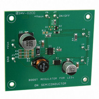
EVAL BOARD FOR NCP3065SOBSTG
Manufacturer
ON Semiconductor
Datasheets
1.NCP3065DR2G.pdf
(18 pages)
2.NCP3065SOBSTGEVB.pdf
(1 pages)
3.NCP3065SOBSTGEVB.pdf
(18 pages)
Specifications of NCP3065SOBSTGEVB
Design Resources
NCP3065 Boost Eval Board BOM NCP3065SOBSTGEVB Gerber Files NCP3065 Boost Eval Board Schematic
Current - Output / Channel
350mA
Outputs And Type
1, Non-Isolated
Voltage - Output
20 V
Voltage - Input
12V
Utilized Ic / Part
NCP3065
Core Chip
NCP3065
Topology
Buck-Boost
No. Of Outputs
1
Dimming Control Type
PWM
Development Tool Type
Hardware - Eval/Demo Board
Leaded Process Compatible
Yes
Mcu Supported Families
NCP3065
Rohs Compliant
Yes
Lead Free Status / RoHS Status
Lead free / RoHS Compliant
Features
-
Lead Free Status / Rohs Status
Lead free / RoHS Compliant
For Use With/related Products
NCP3065SOBSTG
Other names
NCP3065SOBSTGEVBOS


The duty cycle is defined as
The input ripple current is defined as
The load voltage must always be higher than the input
voltage. This voltage is defined as
where V
reference voltage, and n = number of LED’s in cluster.
of load voltage variation, a sense resistor is placed across the
feedback voltage. This drop is calculated as
The V
feedback comparator threshold.
Simple Boost 350 mA LED driver
driver is shown in Figure 22. It is well suited to automotive
or industrial applications where limited board space and a
high voltage and high ambient temperature range might be
found. The NCP3065 also incorporates safety features such
as peak switch current and thermal shutdown protection.
The schematic has an external high side current sense
resistor that is used to detect if the peak current is exceeded.
In the constant current configuration, protection is also
required in the event of an open LED fault since current will
continue to charge the output capacitor causing the output
voltage to rise. An external zener diode is used to clamp the
output voltage in this fault mode. Although the NCP3065 is
designed to operate up to 40 V additional input transient
protections might be required in certain automotive
applications due to inductive load dump.
external capacitor C4. The t
internal feedback comparator, peak current comparator and
main oscillator. The output current is configured by an
internal feedback comparator with negative feedback input.
The positive input is connected to an internal voltage
reference of 0.235 V with 10% precision over temperature.
The nominal LED current is setup by a feedback resistor.
This current is defined as:
Both use the negative comparator input as a shutdown input.
When the pin voltage is higher than 0.235 V the switch
When operating in CCM the output voltage is equal to
Since the converter needs to regulate current independent
The NCP3065 boost converter is configured as a LED
The main operational frequency is determined by the
There are two approaches to implement LED dimming.
sense
V
D +
DI + V
V
V
I
OUT
f
OUT
load
sense
= LED forward voltage, V
corresponds to the internal voltage reference or
t
+
+ V
ON
+ V
+ I
IN
R
0.235
t
) t
f * L
ON
sense
sense
IN
load
D
OFF
@
) n * R
1 * D
) n * V
+
1
t
ON
T
sense
on
f
time is controlled by the
sense
is the converter
http://onsemi.com
16
transistor is off. You could connect an external PWM signal
to pin ON/OFF and a power source to pin +V
the PWM dimming function. When the dimming signal
exceeds the turn on threshold of the external PNP or NPN
transistor, the comp pin will be pulled up. A TTL level input
can also be used for dimming control. The range of the
dimming frequency is from 100 Hz to 1 kHz, but it is
recommended to use frequency around 200 Hz as this is
safely above the frequency where the human eye can detect
the pulsed behavior, in addition this value is convenient to
minimize EMI. There are two options to determine the
dimming polarity. The first one uses the NPN switching
transistor and the second uses a PNP switching transistor.
The switch on/off level is dependent upon the chosen
dimming topology. The external voltage source (V
should have a voltage ranging from +5 V
Figure 17 illustrates average LEDs current dependency on
the dimming input signal duty cycle.
comparator is used which has a nominal 200 mV threshold.
The value of resistor R1 determines the current limit value
and is configured according to the following equation.
The maximum output voltage is clamped with an external
zener diode, D2 with a value of 36 V which protects the
NCP3065 output from an open LED fault.
needs. You can use one 150 mW (R1) or a combination of
parallel resistors such as six 1 W resistors (R2 − R7) for
current sense.
LEDs with a typical V
in several serial combinations (4, 6, 8 LED’s string) and
4 chip and 6 chip LEDs with V
20.8 V @ 700 mA.
voltage and input current and LED current and LED voltage
drop. The output current is dependent on the peak current,
inductor value, input voltage and voltage drop value and of
course on the switching frequency.
For cycle by cycle switch current limiting a second
The demo board has a few options to configure it to your
To evaluate the functionality of the board, high power
The efficiency was calculated by measuring the input
D +
I
Number of LEDs
OUT
I
+ (D * D
V
pk(SW)
OUT
V
4
6
8
OUT
) V
+
) V
0.15
0.2
F
2
) *
* V
F
* V
f
+ 1.33 A
= 3.42 V @ 350 mA were connected
I
SWCE
pk(SW)
IN
String Forward Voltage at 255C
16.74
22.32
D
11.16
Min
[*]
*
f
V
=14V respectively V
IN
2 * L * f
* V
13.68
20.52
27.36
Typ
SWCE
AUX
DC
[A]
to realize
to +V
15.96
23.94
31.92
Max
AUX
f
IN
=
)
.
Related parts for NCP3065SOBSTGEVB
Image
Part Number
Description
Manufacturer
Datasheet
Request
R

Part Number:
Description:
Up to 1.5 A Constant Current Switching Regulator for LEDs
Manufacturer:
ON Semiconductor
Datasheet:

Part Number:
Description:
EVAL BOARD FOR NCP3065SOBCKG
Manufacturer:
ON Semiconductor
Datasheet:

Part Number:
Description:
EVAL BOARD FOR NCP30653ABCKG
Manufacturer:
ON Semiconductor
Datasheet:
Part Number:
Description:
ON Semiconductor [VOLTAGE REGULATOR]
Manufacturer:
ON Semiconductor
Datasheet:
Part Number:
Description:
357-036-542-201 CARDEDGE 36POS DL .156 BLK LOPRO
Manufacturer:
ON Semiconductor
Datasheet:
Part Number:
Description:
357-036-542-201 CARDEDGE 36POS DL .156 BLK LOPRO
Manufacturer:
ON Semiconductor
Datasheet:
Part Number:
Description:
357-036-542-201 CARDEDGE 36POS DL .156 BLK LOPRO
Manufacturer:
ON Semiconductor
Datasheet:
Part Number:
Description:
357-036-542-201 CARDEDGE 36POS DL .156 BLK LOPRO
Manufacturer:
ON Semiconductor
Datasheet:
Part Number:
Description:
357-036-542-201 CARDEDGE 36POS DL .156 BLK LOPRO
Manufacturer:
ON Semiconductor
Datasheet:
Part Number:
Description:
357-036-542-201 CARDEDGE 36POS DL .156 BLK LOPRO
Manufacturer:
ON Semiconductor
Datasheet:
Part Number:
Description:
357-036-542-201 CARDEDGE 36POS DL .156 BLK LOPRO
Manufacturer:
ON Semiconductor
Datasheet:
Part Number:
Description:
357-036-542-201 CARDEDGE 36POS DL .156 BLK LOPRO
Manufacturer:
ON Semiconductor
Datasheet:
Part Number:
Description:
357-036-542-201 CARDEDGE 36POS DL .156 BLK LOPRO
Manufacturer:
ON Semiconductor
Datasheet:
Part Number:
Description:
357-036-542-201 CARDEDGE 36POS DL .156 BLK LOPRO
Manufacturer:
ON Semiconductor
Datasheet: