EVAL-ADUC824QS Analog Devices Inc, EVAL-ADUC824QS Datasheet - Page 23
EVAL-ADUC824QS
Manufacturer Part Number
EVAL-ADUC824QS
Description
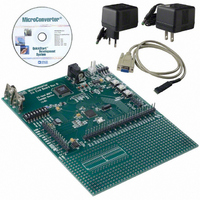
KIT DEV FOR ADUC824 QUICK START
Manufacturer
Analog Devices Inc
Series
QuickStart™ Kitr
Type
8052-corer
Datasheet
1.EVAL-ADUC824QSZ.pdf
(68 pages)
Specifications of EVAL-ADUC824QS
Contents
Evaluation Board, Power Supply, Cable, Software and Documentation
For Use With/related Products
ADuC824
Lead Free Status / RoHS Status
Contains lead / RoHS non-compliant


The SFR space is mapped to the upper 128 bytes of internal data
memory space and accessed by direct addressing only. It provides
an interface between the CPU and all on-chip peripherals. A block
diagram showing the programming model of the ADuC824 via
the SFR area is shown in Figure 16. A complete SFR map is shown
in Figure 17.
OVERVIEW OF MCU-RELATED SFRs
Accumulator SFR
ACC is the Accumulator register and is used for math operations
including addition, subtraction, integer multiplication and division,
and Boolean bit manipulations. The mnemonics for accumulator-
specific instructions refer to the Accumulator as A.
B SFR
The B register is used with the ACC for multiplication and divi-
sion operations. For other instructions it can be treated as a
general-purpose scratchpad register.
Stack Pointer SFR
The SP register is the stack pointer and is used to hold an internal
RAM address that is called the ‘top of the stack.’ The SP register is
incremented before data is stored during PUSH and CALL execu-
tions. While the stack may reside anywhere in on-chip RAM, the
SP register is initialized to 07H after a reset. This causes the
stack to begin at location 08H.
Data Pointer
The Data Pointer is made up of three 8-bit registers, named
DPP (page byte), DPH (high byte), and DPL (low byte).
These are used to provide memory addresses for internal and
external code access and external data access. It may be ma-
nipulated as a 16-bit register (DPTR = DPH, DPL), although
INC DPTR instructions will automatically carry over to DPP, or
as three independent 8-bit registers (DPP, DPH, DPL).
FLASH/EE PROGRAM
REPROGRAMMABLE
ELECTRICALLY
COMPATIBLE
NONVOLATILE
256 BYTES
MEMORY
8 KBYTE
CORE
8051-
RAM
FUNCTION
REGISTER
128-BYTE
SPECIAL
AREA
REPROGRAMMABLE
SIGMA-DELTA ADCs
FLASH/EE DATA
OTHER ON-CHIP
ELECTRICALLY
TEMPERATURE
NONVOLATILE
PERIPHERALS
12-BIT DAC
SERIAL I/O
SOURCES
CURRENT
640-BYTE
MEMORY
SENSOR
DUAL
WDT
PSM
PLL
TIC
Program Status Word SFR
The PSW register is the Program Status Word which contains
several bits reflecting the current status of the CPU as detailed in
Table I.
SFR Address
Power ON Default Value
Bit Addressable
Bit
7
6
5
4
3
2
1
0
Power Control SFR
The Power Control (PCON) register contains bits for power-
saving options and general-purpose status flags as shown in
Table II.
SFR Address
Power ON Default Value
Bit Addressable
Bit
7
6
5
4
3
2
1
0
S
C
M
O
Y
D
S
E
A
R
C
I
Table II. PCON SFR Bit Designations
P
Table I. PSW SFR Bit Designations
Name
CY
AC
F0
RS1
RS0
OV
F1
P
Name
SMOD
SERIPD
INT0PD
ALEOFF
GF1
GF0
PD
IDL
D
I
N
F
T
0
0
P
D
A
R
L
E
S
O
1
F
F
Description
Carry Flag
Auxiliary Carry Flag
General-Purpose Flag
Register Bank Select Bits
RS1
0
0
1
1
Overflow Flag
General-Purpose Flag
Parity Bit
Description
Double UART Baud Rate
I
Enable
INT0 Power-Down Interrupt
Enable
Disable ALE Output
General-Purpose Flag Bit
General-Purpose Flag Bit
Power-Down Mode Enable
Idle Mode Enable
2
C/SPI Power-Down Interrupt
R
G
S
F
D0H
No
00H
Yes
87H
00H
1
0
RS0
0
1
0
1
O
G
F
V
0
ADuC824
Selected Bank
0
1
2
3
F
P
D
1
I
P
D
L
Related parts for EVAL-ADUC824QS
Image
Part Number
Description
Manufacturer
Datasheet
Request
R


Part Number:
Description:
BOARD EVAL FOR SI270X-A
Manufacturer:
Silicon Laboratories Inc
Datasheet:

Part Number:
Description:
BUCK CONV REF DESIGN KIT IP1201
Manufacturer:
International Rectifier
Datasheet:
Part Number:
Description:
BOARD DEMO SYNC DUAL BUCK CNVTER
Manufacturer:
International Rectifier
Datasheet:
Part Number:
Description:
BOARD DEMO SYNC BUCK CONVETER
Manufacturer:
International Rectifier
Datasheet:

Part Number:
Description:
EVALBOARD/EB Omnidirectional microphone - Analog
Manufacturer:
Analog Devices
Datasheet:
Part Number:
Description:
EVALBOARD/EB Omnidirectional microphone - Analog
Manufacturer:
Analog Devices
Datasheet:


Part Number:
Description:
BOARD EVAL LED DRIVER LT3756
Manufacturer:
Linear Technology
Datasheet:

Part Number:
Description:
BOARD EVAL FOR AD7741/7742
Manufacturer:
Analog Devices Inc
Datasheet:

Part Number:
Description:
±1.7g Dual-Axis IMEMS Accelerometer Evaluation Board
Manufacturer:
Analog Devices Inc
Datasheet:

Part Number:
Description:
IC MULTIPLIER ANALOG 8-SOIC T/R
Manufacturer:
Analog Devices Inc
Datasheet:

Part Number:
Description:
IC ANALOG MULTIPLIER 8-DIP
Manufacturer:
Analog Devices Inc
Datasheet:
Part Number:
Description:
IC ANALOG MULTIPLIER 8-SOIC
Manufacturer:
Analog Devices Inc
Datasheet:
Part Number:
Description:
IC ANALOG MULTIPLIER 8-DIP
Manufacturer:
Analog Devices Inc
Datasheet: