EVAL-ADUC824QS Analog Devices Inc, EVAL-ADUC824QS Datasheet - Page 51
EVAL-ADUC824QS
Manufacturer Part Number
EVAL-ADUC824QS
Description
KIT DEV FOR ADUC824 QUICK START
Manufacturer
Analog Devices Inc
Series
QuickStart™ Kitr
Type
8052-corer
Datasheet
1.EVAL-ADUC824QSZ.pdf
(68 pages)
Specifications of EVAL-ADUC824QS
Contents
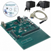
Evaluation Board, Power Supply, Cable, Software and Documentation
For Use With/related Products
ADuC824
Lead Free Status / RoHS Status
Contains lead / RoHS non-compliant


8051-COMPATIBLE ON-CHIP PERIPHERALS
This section gives a brief overview of the various secondary periph-
eral circuits are also available to the user on-chip. These remaining
functions are fully 8051-compatible and are controlled via standard
8051 SFR bit definitions.
Parallel I/O Ports 0–3
The ADuC824 uses four input/output ports to exchange data with
external devices. In addition to performing general-purpose I/O,
some ports are capable of external memory operations; others are
multiplexed with an alternate function for the peripheral features
on the device. In general, when a peripheral is enabled, that pin
may not be used as a general purpose I/O pin.
Port 0 is an 8-bit open drain bidirectional I/O port that is directly
controlled via the Port 0 SFR (SFR address = 80 hex). Port 0
pins that have 1s written to them via the Port 0 SFR will be
configured as open drain and will therefore float. In that state,
Port 0 pins can be used as high impedance inputs. An external
pull-up resistor will be required on Port 0 outputs to force a
valid logic high level externally. Port 0 is also the multiplexed
low-order address and data bus during accesses to external pro-
gram or data memory. In this application it uses strong internal
pull-ups when emitting 1s.
Port 1 is also an 8-bit port directly controlled via the P1 SFR
(SFR address = 90 hex). The Port 1 pins are divided into two
distinct pin groupings.
P1.0 and P1.1 pins on Port 1 are bidirectional digital I/O pins with
internal pull-ups. If P1.0 and P1.1 have 1s written to them via the
P1 SFR, these pins are pulled high by the internal pull-up resis-
tors. In this state they can also be used as inputs; as input pins
being externally pulled low, they will source current because of
the internal pull-ups. With 0s written to them, both these pins
will drive a logic low output voltage (VOL) and will be capable of
sinking 10 mA compared to the standard 1.6 mA sink capa-
bility on the other port pins. These pins also have various
secondary functions described in Table XXI.
Pin
P1.0
P1.1
The remaining Port 1 pins (P1.2–P1.7) can only be configured
as Analog Input (ADC), Analog Output (DAC) or Digital Input
pins. By (power-on) default these pins are configured as Analog
Inputs, i.e., ‘1’ written in the corresponding Port 1 register bit.
To configure any of these pins as digital inputs, the user should
write a ‘0’ to these port bits to configure the corresponding pin
as a high impedance digital input.
Port 2 is a bidirectional port with internal pull-up resistors directly
controlled via the P2 SFR (SFR address = A0 hex). Port 2 pins
that have 1s written to them are pulled high by the internal pull-up
resistors and, in that state, they can be used as inputs. As inputs,
Port 2 pins being pulled externally low will source current because
of the internal pull-up resistors. Port 2 emits the high order
address bytes during fetches from external program memory
and middle and high order address bytes during accesses to the
24-bit external data memory space.
Table XXI. Port 1, Alternate Pin Functions
Alternate Function
T2 (Timer/Counter 2 External Input)
T2EX (Timer/Counter 2 Capture/Reload Trigger)
Port 3 is a bidirectional port with internal pull-ups directly
controlled via the P2 SFR (SFR address = B0 hex). Port 3 pins
that have 1s written to them are pulled high by the internal pull-ups
and in that state they can be used as inputs. As inputs, Port 3
pins being pulled externally low will source current because of the
internal pull-ups. Port 3 pins also have various secondary func-
tions described in Table XXII.
Pin
P3.0
P3.1
P3.2
P3.3
P3.4
P3.5
P3.6
P3.7
The alternate functions of P1.0, P1.1, and Port 3 pins can only be
activated if the corresponding bit latch in the P1 and P3 SFRs
contains a 1. Otherwise, the port pin is stuck at 0.
Timers/Counters
The ADuC824 has three 16-bit Timer/Counters: Timer 0,
Timer 1, and Timer 2. The Timer/Counter hardware has been
included on-chip to relieve the processor core of the overhead
inherent in implementing timer/counter functionality in soft-
ware. Each Timer/Counter consists of two 8-bit registers THx and
TLx (x = 0, 1, and 2). All three can be configured to operate
either as timers or event counters.
In ‘Timer’ function, the TLx register is incremented every machine
cycle. Thus one can think of it as counting machine cycles. Since a
machine cycle consists of 12 core clock periods, the maximum
count rate is 1/12 of the core clock frequency.
In ‘Counter’ function, the TLx register is incremented by a 1-to-0
transition at its corresponding external input pin, T0, T1, or T2.
In this function, the external input is sampled during S5P2 of
every machine cycle. When the samples show a high in one cycle
and a low in the next cycle, the count is incremented. The new
count value appears in the register during S3P1 of the cycle follow-
ing the one in which the transition was detected. Since it takes two
machine cycles (24 core clock periods) to recognize a 1-to-0 transi-
tion, the maximum count rate is 1/24 of the core clock frequency.
There are no restrictions on the duty cycle of the external input
signal, but to ensure that a given level is sampled at least once
before it changes, it must be held for a minimum of one full machine
cycle. Remember that the core clock frequency is programmed
via the CD0–2 selection bits in the PLLCON SFR.
Table XXII. Port 3, Alternate Pin Functions
Alternate Function
RXD (UART Input Pin)
(or Serial Data I/O in Mode 0)
TXD (UART Output Pin)
(or Serial Clock Output in Mode 0)
INT0 (External Interrupt 0)
INT1 (External Interrupt 1)
T0 (Timer/Counter 0 External Input)
T1 (Timer/Counter 1 External Input)
WR (External Data Memory Write Strobe)
RD (External Data Memory Read Strobe)
ADuC824
Related parts for EVAL-ADUC824QS
Image
Part Number
Description
Manufacturer
Datasheet
Request
R


Part Number:
Description:
BOARD EVAL FOR SI270X-A
Manufacturer:
Silicon Laboratories Inc
Datasheet:

Part Number:
Description:
BUCK CONV REF DESIGN KIT IP1201
Manufacturer:
International Rectifier
Datasheet:
Part Number:
Description:
BOARD DEMO SYNC DUAL BUCK CNVTER
Manufacturer:
International Rectifier
Datasheet:
Part Number:
Description:
BOARD DEMO SYNC BUCK CONVETER
Manufacturer:
International Rectifier
Datasheet:

Part Number:
Description:
EVALBOARD/EB Omnidirectional microphone - Analog
Manufacturer:
Analog Devices
Datasheet:
Part Number:
Description:
EVALBOARD/EB Omnidirectional microphone - Analog
Manufacturer:
Analog Devices
Datasheet:


Part Number:
Description:
BOARD EVAL LED DRIVER LT3756
Manufacturer:
Linear Technology
Datasheet:

Part Number:
Description:
BOARD EVAL FOR AD7741/7742
Manufacturer:
Analog Devices Inc
Datasheet:

Part Number:
Description:
±1.7g Dual-Axis IMEMS Accelerometer Evaluation Board
Manufacturer:
Analog Devices Inc
Datasheet:

Part Number:
Description:
IC MULTIPLIER ANALOG 8-SOIC T/R
Manufacturer:
Analog Devices Inc
Datasheet:

Part Number:
Description:
IC ANALOG MULTIPLIER 8-DIP
Manufacturer:
Analog Devices Inc
Datasheet:
Part Number:
Description:
IC ANALOG MULTIPLIER 8-SOIC
Manufacturer:
Analog Devices Inc
Datasheet:
Part Number:
Description:
IC ANALOG MULTIPLIER 8-DIP
Manufacturer:
Analog Devices Inc
Datasheet: